- 신규로 표시
- 북마크
- 구독
- 소거
- RSS 피드 구독
- 강조
- 인쇄
- 부적절한 컨텐트 신고
We are using an Arria 10 device, 10AS057N2F40E2SG, with some JESD204 Receive only channels.
The ADC being used is the T.I. ADC09QJ800AAV in JMODE = 2 (for 4 lanes, 8b/10b).
I have a XCVR reset controller instantiated in the QSYS design along with the JESD itself plus a few other things - extremely similar to the Intel design example for JESD.
On further inspection I found that one of the four rx_is_lockedtodata signals is deactivated, causing the various outputs such as rx_ready to be deactivated, and rx_digitalreset to be activated.
The rx_analogreset outputs are remaining low.
The particular one of the four rx_is_lockedtodata that is lost seems to be almost random.
What could be the cause of this regular event?
Thanks
David
링크가 복사됨
- 신규로 표시
- 북마크
- 구독
- 소거
- RSS 피드 구독
- 강조
- 인쇄
- 부적절한 컨텐트 신고
Hi,
Thanks for contacting Intel. I'm assigned to support request.
I'll investigate on this case related to XXX and get back to you soon once I have any finding.
Meanwhile can I check with you on:
1. Quartus Version
2. Custom design or example design
3. JESD204B or C?
Thanks for your patience.
Best regards,
Harsh M
- 신규로 표시
- 북마크
- 구독
- 소거
- RSS 피드 구독
- 강조
- 인쇄
- 부적절한 컨텐트 신고
Hi Harshx.
1. PRO 23.4
2. Custom but very heavily relying on copying from example design.
3. 204B.
Thanks
David
- 신규로 표시
- 북마크
- 구독
- 소거
- RSS 피드 구독
- 강조
- 인쇄
- 부적절한 컨텐트 신고
Hi,
Can you check your board (Arria10) with an example design?
Since rx_is_lockedtodata is deactivated have you checked TX side for all lanes ?
Is it possible for you to share a block diagram for better understanding about your design and connections.
Regards,
Harsh M
- 신규로 표시
- 북마크
- 구독
- 소거
- RSS 피드 구독
- 강조
- 인쇄
- 부적절한 컨텐트 신고
Hi Harsh
1. I could not generate an example design that is matching the particular TX (ADC from TI).
2. Pretty hard to check since lanes are internal PCB layers and the assembly structure does not let us probe so easily.
3. I can share all information such as parts of the schematic and also the FPGA design. Which ones do you want?
David
- 신규로 표시
- 북마크
- 구독
- 소거
- RSS 피드 구독
- 강조
- 인쇄
- 부적절한 컨텐트 신고
Hi,
Kindly refer this: Solved: Why are signals rx_is_locktodata and rx_is_locktoref always at 0? - Intel Community
Kindly check the attached design as well, its similar to your case.
Let me know the results (or you face any issues).
Thanks
Regards,
Harsh M
- 신규로 표시
- 북마크
- 구독
- 소거
- RSS 피드 구독
- 강조
- 인쇄
- 부적절한 컨텐트 신고
Hi Harsh,
I took a quick look at the project linked.
That is a transmitter only, whereas I am using receiver only.
But that did give me an idea, i.e. of making a design with the bare bones receiver and only once that is working, continue on to full JESD.
Would you recommend for to instantiate all the parts manually (such as the TX PHY, TX PHY Reset controller, etc ) and individually or does some top level wrapper already exist?
In my original design (using the above-mentioned ADC from T.I.) each ADC part outputs a low-jitter replica of the internal sampling clock. This clock then forms the reference clock input to the JESD receiver / PLL.
In the bare PHY test that I will do, I assume that the correct PLL to use it the ATX PLL. Is this correct?
Thanks
David
- 신규로 표시
- 북마크
- 구독
- 소거
- RSS 피드 구독
- 강조
- 인쇄
- 부적절한 컨텐트 신고
Hello Harsh,
I just noticed this quote from the ug_arria10_xcvr_phy-683617-666805.pdf document:

In my design, CLKUSR (100MHZ) is always stable before the FPGA is configured.
However, the JESD reference clock input to the PLL in the transceiver bank is sourced by the ADC.
The ADC is only configured AFTER the FPGA is configured, since FPGA logic is used to master the ADC SPI bus.
So, is this quote from the document above a hard requirement?
If it is, then I would have find a way to configure twice.
The first would enable the ADC clock output, and the second configuration cycle would be the one where transceiver does it's calibration.
Thanks
David
- 신규로 표시
- 북마크
- 구독
- 소거
- RSS 피드 구독
- 강조
- 인쇄
- 부적절한 컨텐트 신고
Thanks for this info Harsh.
It will take me some time to be able to test this.
Please either leave this thread open for about a month or maybe I will just re-open it once I have progressed a bit.
David
- 신규로 표시
- 북마크
- 구독
- 소거
- RSS 피드 구독
- 강조
- 인쇄
- 부적절한 컨텐트 신고
Hello Harsh,
I have modified the environment so now the reference clock to the JESD receiver is stable when the FPGA comes out of configuration.
On Signal Tap I am still seeing that the rx_is_lockedtodata signals (I have 4 lanes in my device) randomly toggle.
In the first attached screenshot you can see that all signals become locked and then the digital resets become inactivated.
In the second screenshot I show the opposite, when one of rx_is_lockedtodata becomes false causing the reset to become active.
How can I proceed to tackle this problem?
Thanks
David
- 신규로 표시
- 북마크
- 구독
- 소거
- RSS 피드 구독
- 강조
- 인쇄
- 부적절한 컨텐트 신고
Hi Harsh,
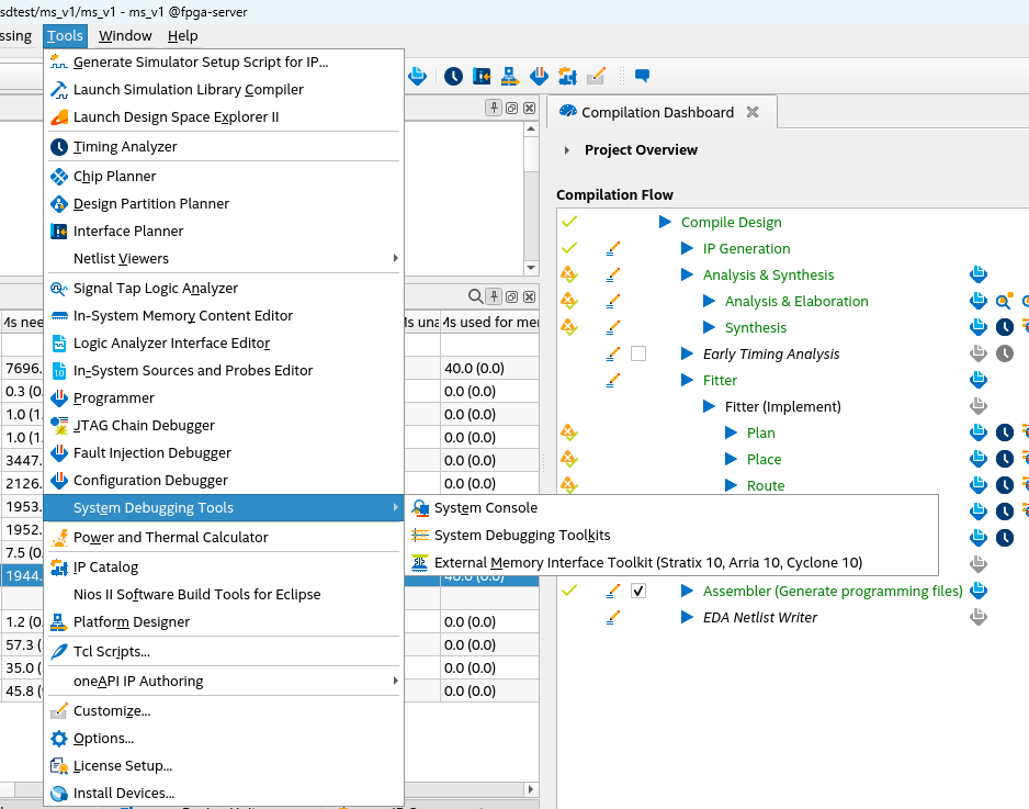
I thought of using the Transceiver Toolkit to help track down the problem.
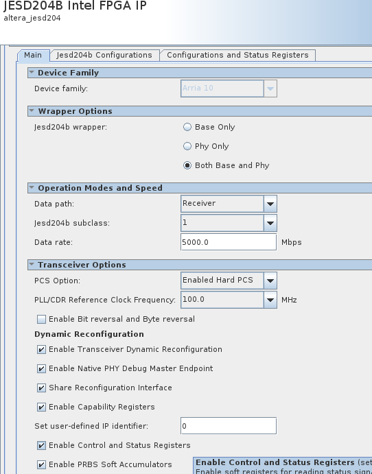
I made sure that all the necessary options in the JESD IP were enabled (dynamic reconfiguration, etc), and connected the signals in QSYS to a JTAG Master.
The JTAG Master is recognized in System Console but the Toolkit does not recognize any debug endpoint.
Could you please also help with this.
Thanks
David
- 신규로 표시
- 북마크
- 구독
- 소거
- RSS 피드 구독
- 강조
- 인쇄
- 부적절한 컨텐트 신고
Hi,
Do you have any error messages in the "messages" window?
What do you mean by "The JTAG Master is recognized in System Console but Toolkit does not recognize any debug endoiint" ?
The design is loading properly? and is in reset or not?
Regards,
Harsh M
- 신규로 표시
- 북마크
- 구독
- 소거
- RSS 피드 구독
- 강조
- 인쇄
- 부적절한 컨텐트 신고
- 신규로 표시
- 북마크
- 구독
- 소거
- RSS 피드 구독
- 강조
- 인쇄
- 부적절한 컨텐트 신고
Hi David,
Ya sure you can share the description with screenshots.
No other information is needed.
Regards,
Harsh M
- 신규로 표시
- 북마크
- 구독
- 소거
- RSS 피드 구독
- 강조
- 인쇄
- 부적절한 컨텐트 신고
Hello Harsh,
Some screenshots as follows:
1. jesd_toolkit_setup: shows that I have enabled the toolkit in Platform Designer
2. from_system_console: shows that the JTAG master is recognized
3. no_XCVR_toolkit_available: however no toolkit is available
Basically the flow is:
1. Program the SOF
2. Use ISSP Source to trigger a module within FPGA that configures the clock generator on the board to start making clocks
3. Use System Console to configure the ADC (JESD mode, PLL etc)
4. Program the SOF again. This is to ensure that the FPGA exits it's configuration phase when the input transceiver reference clock and JESD lanes are active
5. check SYNC_N from JESD IP (always low)
6. reset JESD IP
7. check SYNC_N from JESD IP (always low)
That's it.
Any help appreciated.
David