- Mark as New
- Bookmark
- Subscribe
- Mute
- Subscribe to RSS Feed
- Permalink
- Report Inappropriate Content
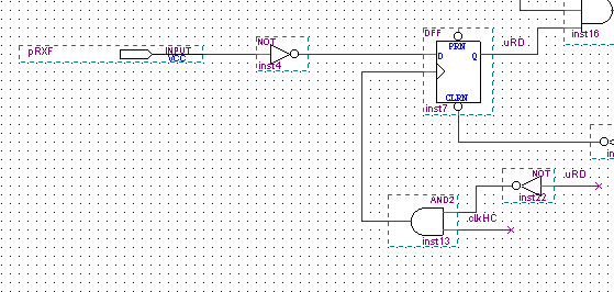
it is possible that quartus connect external pin to clock via not (inst13)
- Thank you
- Regaerd.
Link Copied
- Mark as New
- Bookmark
- Subscribe
- Mute
- Subscribe to RSS Feed
- Permalink
- Report Inappropriate Content
Hello,
Yes, you can choose an external clock, you can assign your signal to the external pin clock into the pin planner.
If you need more help, please provide the board that you are using!
Best regards,
Isaac Vazquez
- Mark as New
- Bookmark
- Subscribe
- Mute
- Subscribe to RSS Feed
- Permalink
- Report Inappropriate Content
Hello, did this info works for you?
Best regards!
- Mark as New
- Bookmark
- Subscribe
- Mute
- Subscribe to RSS Feed
- Permalink
- Report Inappropriate Content
when clock are dircet input pin i have this message :
Warning: Can't achieve minimum setup and hold requirement RXFn along 24 path(s). See Report window for details
also i do see in attachment
I have another message
Warning: Can't achieve minimum setup and hold requirement clk32 along 696 path(s). See Report window for details
My clock provide fromp 3,3v 33Mhz oscillator connected at input clock (ep3c5)
Regard
- Mark as New
- Bookmark
- Subscribe
- Mute
- Subscribe to RSS Feed
- Permalink
- Report Inappropriate Content
Hello,
which is the purpose of the not (inst4)? Can you try your design without the not?
If this didn't work, can you provide me your design to work on the debug?
Best regards!
- Mark as New
- Bookmark
- Subscribe
- Mute
- Subscribe to RSS Feed
- Permalink
- Report Inappropriate Content
Hello,
Did you find the solution? if you still having the same issue, can you share your design?
Bestregards,
Isaac Vazquez.
- Mark as New
- Bookmark
- Subscribe
- Mute
- Subscribe to RSS Feed
- Permalink
- Report Inappropriate Content
Hello and thank you very much for your email
Sorry for the delay in my response.
Let's say that I partially manage to advance my design.
After a compilation my design works, then after another modification and compilation my design does not work anymore.
When the design was simple it worked well. Currently the design is becoming complex, about 85% of the FPGA gates are used. I also watch the compiltation time which increases with the complexity of the design. My computer is not fast, it takes patience.
The FPGA I am using is an EP3-C5 / 10.
In my board I use a 33MHz oscillator supplied with 3v3.
It is connected to the clock0 pin of the FPGA via a 33 Ω series resistor. To obtain a multitude of frequencies I used a simple divider counter which divides by 24 the clock of the oscillator.
I also use a PLL but the function which is fed by the signals of this PLL does not work.
I have read on various forums and documentation that clocks and signals should be synchronous.
Would there be a tutorial in French which simply explains the management of clocks and signals.
Is this synchronization valid for low frequency signals for example a few hertz at 5 kilohertz ?
Thank you for your understanding.
Regard
- Mark as New
- Bookmark
- Subscribe
- Mute
- Subscribe to RSS Feed
- Permalink
- Report Inappropriate Content
Hello,
There is no info in French, you can have information in Japanese, Chinese or English.
You can find more info about clock management here: https://www.intel.com/content/dam/www/programmable/us/en/pdfs/literature/hb/cyc3/cyc3_ciii51006.pdf
Best regards.
- Mark as New
- Bookmark
- Subscribe
- Mute
- Subscribe to RSS Feed
- Permalink
- Report Inappropriate Content
Hello
Very thank for your replies.
I posted this subject on your forums: multiple clocks from 1 pin dedicated clock. Looks like sstrell helped me as well.
Currently I am busy understanding the "timequest" function .
How to identify and quantify time problems .
How to provide information to Quartus, Timequest to correct problems .
I'm just starting to handle the "sdc" type file
Thank you for your answers.
Best regards.
- Subscribe to RSS Feed
- Mark Topic as New
- Mark Topic as Read
- Float this Topic for Current User
- Bookmark
- Subscribe
- Printer Friendly Page