- Mark as New
- Bookmark
- Subscribe
- Mute
- Subscribe to RSS Feed
- Permalink
- Report Inappropriate Content
Dear,
10M08SCU169I7G with vccio1B=1.8v; vccio8=3.3V (vccio1a=2.5v)Configuration pins are in banks 1B + 8
Quartus prime 18.0 standard build 614
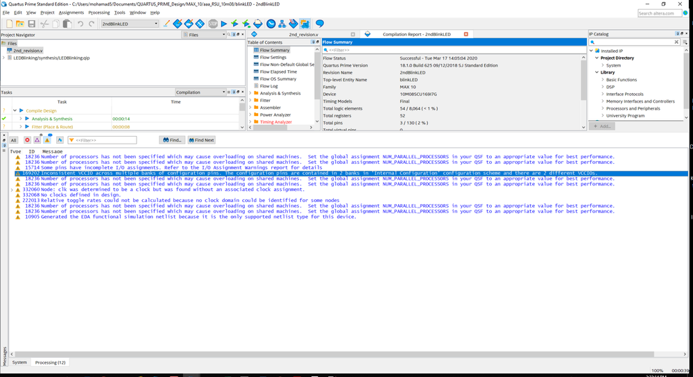
Warning (169202): Inconsistent VCCIO across multiple banks of configuration pins. The configuration pins are contained in 2 banks in 'Internal Configuration' configuration scheme and there are 2 different VCCIOs.
Regards,
Stefan
Link Copied
- Mark as New
- Bookmark
- Subscribe
- Mute
- Subscribe to RSS Feed
- Permalink
- Report Inappropriate Content
Hi Stefan,
The problem of this warning ID because the configuration pins are powered by different Vccio in different banks.
Solution: Enforce a configuration voltage level in the Configuration tab
Cheers
- Mark as New
- Bookmark
- Subscribe
- Mute
- Subscribe to RSS Feed
- Permalink
- Report Inappropriate Content
Hello Shafiq,
Pin-planner signal list shows vccio1b=1.8 and vccio8=3.3 because I defined these io-standards on their signals in assignment-editor.
assignments > device > device and pin options > configuration : in this screen I tried with box checked/unchecked "Force Vccio to be compatible with configuration IO-voltage: but this gives no difference .... I don't see anything else I that relates to Vccio 0 config pins ? ?
Regards,
Stefan
- Mark as New
- Bookmark
- Subscribe
- Mute
- Subscribe to RSS Feed
- Permalink
- Report Inappropriate Content
Hi Stefan,
The issue is the configuration pins are powered by different Vccio.
Have you tried use the same voltage for I/O bank 1B and I/O bank 8? If yes, is it able to solve the issue?
Thanks
- Mark as New
- Bookmark
- Subscribe
- Mute
- Subscribe to RSS Feed
- Permalink
- Report Inappropriate Content
- Mark as New
- Bookmark
- Subscribe
- Mute
- Subscribe to RSS Feed
- Permalink
- Report Inappropriate Content
Hi Stefan,
I'm apologize to take so much time to get the confirmation regarding to this issue. I tested on my side and get the further confirmation from my colleague.
The rule of thumb: The VCCIO for bank 1B (bank 1 for 10M02 devices) and bank 8 must be powered up to a voltage between 1.5V – 3.3V during configuration.
Thus, as long as your Bank 1B & Bank 8 is powered up between that range, you are allowed to have different voltage or same voltage.
When I did the duplication on my side, I also got the same warning as yours:
Actually the warning that you get[Warning (169202)], is the false warning from Quartus. Quartus software Team will fixed it this false warning in future Quartus release.
You may refer to this KDB:
https://www.intel.com/content/www/us/en/programmable/support/support-resources/knowledge-base/tools/2018/-warning--169202---inconsistent-vccio-across-multiple-banks-of-c.html?wapkw=warning%20169202
I'm apologize for inconvenience.
Thanks
- Mark as New
- Bookmark
- Subscribe
- Mute
- Subscribe to RSS Feed
- Permalink
- Report Inappropriate Content
Hello Shafiq, ok issue clarified. I understand this is a false warning and it will be solved in a future Quartus release. By the way I also tried with Quartus19.1 standard edition but false warning is still there.
Regards, Stefan
- Mark as New
- Bookmark
- Subscribe
- Mute
- Subscribe to RSS Feed
- Permalink
- Report Inappropriate Content
Hi Stefan,
The issue has not been solved in Quartus 19.1 standard.
This warning will be remove in a future release of the Quartus standard
I'm apologize for inconvenience.
Thanks
- Mark as New
- Bookmark
- Subscribe
- Mute
- Subscribe to RSS Feed
- Permalink
- Report Inappropriate Content
Hi,
This problem is still present in Quartus 23.1std.1 Build 993 SC Standard Edition.
Regards,
Barbara
- Subscribe to RSS Feed
- Mark Topic as New
- Mark Topic as Read
- Float this Topic for Current User
- Bookmark
- Subscribe
- Printer Friendly Page
