- Отметить как новое
- Закладка
- Подписаться
- Отключить
- Подписка на RSS-канал
- Выделить
- Печать
- Сообщить о недопустимом содержимом
I am Interfacing Intel FPGA Cyclone V (5CEBA5F), MAX V CPLD (5M1270Z) with Flash (S29GL01GT) to configure and store data.
I am using CPLD and Flash device to configure the FPGA. In CPLD, I have implemented PFL IP core to assist the configuration process. During the configuration, data stored in the Flash device are read by CPLD and programmed to FPGA. Configuration of FPGA by CPLD is happening as expected. But during the normal FPGA operation, Flash erase operation fails.
After debugging, I believe that PFL is holding the Flash control and data lines. What is the correct way to instantiate the PFL core in CPLD?
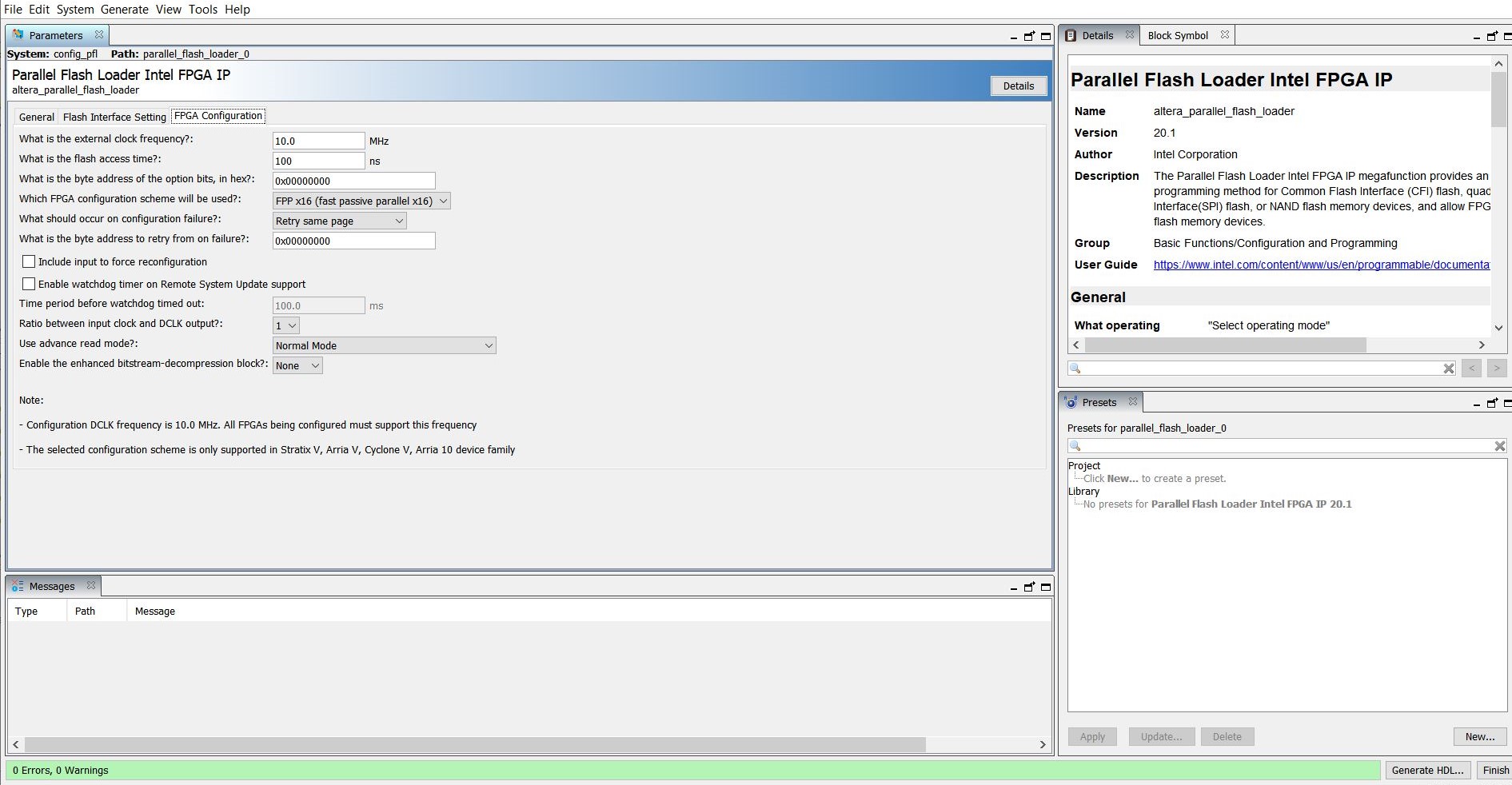
Attached images shows PFL settings.
- Отметить как новое
- Закладка
- Подписаться
- Отключить
- Подписка на RSS-канал
- Выделить
- Печать
- Сообщить о недопустимом содержимом
To reach the solution, I tried following solutions
1) Init_done signal from FPGA is feedback to one of the FPGA's input pin and enable all the FPGA logics AFTER "Init_done" is high.
2) Reset the Flash device after Init_done is high and before writing data to Flash.
3) Use "Flash_ready" signal to verify the Flash state after reset.
I hope this helps.
Ссылка скопирована
- Отметить как новое
- Закладка
- Подписаться
- Отключить
- Подписка на RSS-канал
- Выделить
- Печать
- Сообщить о недопустимом содержимом
Hi,
Thank you for contacting Intel community.
You may refer to PFL IP userguide below:
https://www.intel.com/content/dam/www/programmable/us/en/pdfs/literature/ug/ug_pfl.pdf
Regards,
Aiman
- Отметить как новое
- Закладка
- Подписаться
- Отключить
- Подписка на RSS-канал
- Выделить
- Печать
- Сообщить о недопустимом содержимом
Hi,
If there is no further information needed, I will proceed to close this case.
Thanks.
Regards,
Aiman
- Отметить как новое
- Закладка
- Подписаться
- Отключить
- Подписка на RSS-канал
- Выделить
- Печать
- Сообщить о недопустимом содержимом
To reach the solution, I tried following solutions
1) Init_done signal from FPGA is feedback to one of the FPGA's input pin and enable all the FPGA logics AFTER "Init_done" is high.
2) Reset the Flash device after Init_done is high and before writing data to Flash.
3) Use "Flash_ready" signal to verify the Flash state after reset.
I hope this helps.
- Подписка на RSS-канал
- Отметить тему как новую
- Отметить тему как прочитанную
- Выполнить отслеживание данной Тема для текущего пользователя
- Закладка
- Подписаться
- Страница в формате печати