- Mark as New
- Bookmark
- Subscribe
- Mute
- Subscribe to RSS Feed
- Permalink
- Report Inappropriate Content
Hi,
I am working at implementing a bandpass FIR filter on MAX 10 FPGA development kit. So, I am taking a signal input from the SMA connector into the ADC (1Msps, allowed input clock levels 2, 10, 20, 40, 80Mhz ) followed by a FIR filter block (MATLAB generated HDL) a Parallel to Serial Converter which is connected to the on board DAC (30MHz). Since the DAC has a 24 bit shift register, the clock frequency for ADC and all blocks in between would be 30/24 = 1.25Mhz at max. This not possible with the ADC constraints. The other way around, with 2MHz for the ADC, the DAC would need 48 MHz which is well beyond its maximum range. Where am I going wrong? or is implementing a real time FIR system with these specifications not possible with this board? If not would I have to relax the constraint on DAC and use an external DAC through a PMOD extension? In this case how must i proceed with the design? I'd appreciate any help I can get. Thanks in AdvanceLink Copied
7 Replies
- Mark as New
- Bookmark
- Subscribe
- Mute
- Subscribe to RSS Feed
- Permalink
- Report Inappropriate Content
first you say 1Msps but various clock rates. So I guess your wanted sampling is 1Msps. This means(to me)you are oversampling by 2 f your ADC clock is 2
can't you downsample from 2 to 1 then DAC will be at 24Mhz- Mark as New
- Bookmark
- Subscribe
- Mute
- Subscribe to RSS Feed
- Permalink
- Report Inappropriate Content
--- Quote Start --- first you say 1Msps but various clock rates. So I guess your wanted sampling is 1Msps. This means(to me)you are oversampling by 2 f your ADC clock is 2 can't you downsample from 2 to 1 then DAC will be at 24Mhz --- Quote End --- The maximum sampling rate as per data sheet is 1 Msps. Actually I've tried that, the Qsys Modular ADC gives the fixed clock rates even with different sampling rates. So, 2MHz is the lowest I can go Is there a way around?
- Mark as New
- Bookmark
- Subscribe
- Mute
- Subscribe to RSS Feed
- Permalink
- Report Inappropriate Content
--- Quote Start --- The maximum as per data sheet is 1 Msps. The Qsys Modular ADC gives the mentioned clock rates. How can I down sample ? Could you point me to some resources? --- Quote End --- if your sample rate is 1Msps indeed you have no problem and you don't need downsampling. then your p/s convert will have sample rate of 1Msps at its input, 24 Mbps for DAC. You must sample your data at 1MHz at whatever clock you use (e.g. use clock enable)
- Mark as New
- Bookmark
- Subscribe
- Mute
- Subscribe to RSS Feed
- Permalink
- Report Inappropriate Content
- Mark as New
- Bookmark
- Subscribe
- Mute
- Subscribe to RSS Feed
- Permalink
- Report Inappropriate Content
What does your ADC say about its digital output (you said it gives 1Msps) but what clock does it give you. Remember ADC may have its own internal clock but what matters to you is the clock rate given to you and normally it is same as data rate i.e. 1MHz.
If you have DDR interface it will be 0.5MHz to give you 1Msps- Mark as New
- Bookmark
- Subscribe
- Mute
- Subscribe to RSS Feed
- Permalink
- Report Inappropriate Content
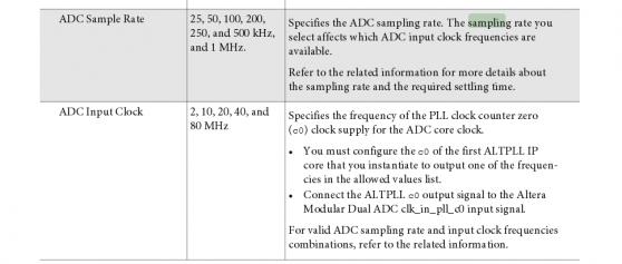
--- Quote Start --- What does your ADC say about its digital output (you said it gives 1Msps) but what clock does it give you. Remember ADC may have its own internal clock but what matters to you is the clock rate given to you and normally it is same as data rate i.e. 1MHz. If you have DDR interface it will be 0.5MHz to give you 1Msps --- Quote End --- Kindly have a look
- Mark as New
- Bookmark
- Subscribe
- Mute
- Subscribe to RSS Feed
- Permalink
- Report Inappropriate Content
the 2,10,20,40 is ADC required clock rate for internal logic. It is not the digital data clock for fpga. I assume you will have a data clock same as sampling rate you choose
Reply
Topic Options
- Subscribe to RSS Feed
- Mark Topic as New
- Mark Topic as Read
- Float this Topic for Current User
- Bookmark
- Subscribe
- Printer Friendly Page