- Mark as New
- Bookmark
- Subscribe
- Mute
- Subscribe to RSS Feed
- Permalink
- Report Inappropriate Content
Hi all
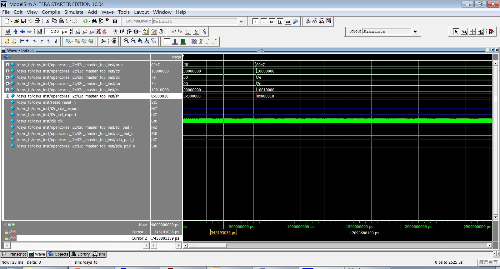
I've downloaded the i2c ip from altera wiki and simulated it in Nios II with ModelSim-Altera. http://www.alterawiki.com/wiki/opencores_i2c (http://www.alterawiki.com/wiki/opencores_i2c) The attached picture is my simulation result. My problem is why the sda and scl are always 0. My C code is basically to enable the i2c ip and to send start condition, address(0x3f), and data.
I2C_init(OPENCORES_I2C_BASE, 100000000, 100000);
I2C_start(OPENCORES_I2C_BASE, 0x3f, 0); // 3f << 1
I2C_write(OPENCORES_I2C_BASE, 3, 0);
I2C_write(OPENCORES_I2C_BASE, 0xf0, 1);
From the simulation result, the prescale register becomes 0x00c7 as expected. (100MHz/5/100KHz-1 = 0x00c7) The register txr becomes 0x7e which stands for the slave address 0x3f and writing operation. The status register shows TIP (transfer in progress) but there's no change on the sda and scl signals. I check "i2c_master_bit_ctrl.v" and find the following code. I guess this is why sda and scal are always 0 but I'm not sure about it.
// assign scl and sda output (always gnd)
assign scl_o = 1'b0;
assign sda_o = 1'b0;
I believe there must be someone who has used this IP successfully. Should I modify the verilog code and is there anything missing in my design?
Link Copied
- Mark as New
- Bookmark
- Subscribe
- Mute
- Subscribe to RSS Feed
- Permalink
- Report Inappropriate Content
You are looking at the wrong signals in your simulation. sda_o and scl_o are in fact tied to ground. The pins are controlled by the respective enable signals. Reading 2.3 external connections in the doc should clarify things,
- Mark as New
- Bookmark
- Subscribe
- Mute
- Subscribe to RSS Feed
- Permalink
- Report Inappropriate Content
Thank FvM for your reply.
I check the signal connections from bottom module to the top module. I think the scl_o and sda_o signals in i2c_master_bit_ctrl module are actually the signals scl_pad_o and sda_pad_o in the top module "opencores_i2c". If the scl_padoen_o and sda_padoen_o are low, scl_pad_o and sda_pad_o are selected as the external output signals. So this is why I check scl_o and sda_o in my simulation.
assign scl_pad_io = scl_padoen_o ? 1'bZ : scl_pad_o;
assign sda_pad_io = sda_padoen_o ? 1'bZ : sda_pad_o;
- Mark as New
- Bookmark
- Subscribe
- Mute
- Subscribe to RSS Feed
- Permalink
- Report Inappropriate Content
I2C is an open-drain protocol, with a pull-up resistor.
scl_padoen_o and sda_padoen_o are only set to '0' when the I2C master needs to transmit a '0'. When it needs to transmit a '1', they're set to '1' and the pin stays in high-Z, letting the pull-up resistor pull the line to '1'. That's why the I2C master designers have hard-wired sda_pad_o and scl_pad_o to '0'. To simulate an I2C bus using Verilog, in addition to that assignment you showed, you need to use "tri1" signals for SCL and SDA. These will go to "weak high" when you drive them to 'Z'.- Mark as New
- Bookmark
- Subscribe
- Mute
- Subscribe to RSS Feed
- Permalink
- Report Inappropriate Content
Hi rbugalho
I learn a lot of things from your reply. Thanks a million.- Mark as New
- Bookmark
- Subscribe
- Mute
- Subscribe to RSS Feed
- Permalink
- Report Inappropriate Content
I have another problem when I use this I2C core to access an EEPROM with a pull high circuit on the SDA and SCL. The problem is why the voltage level of SCL is not stable.
In my attached picture in this reply, the yellow waveform is the SDA signal and the blue waveform is the SCL signal. In the red rectangle, start condition, slave address (7'b1010000), and write operation can be observed.
- Mark as New
- Bookmark
- Subscribe
- Mute
- Subscribe to RSS Feed
- Permalink
- Report Inappropriate Content
Must be some kind of strange hardware. Hard to guess without seeing the full circuit.
- Mark as New
- Bookmark
- Subscribe
- Mute
- Subscribe to RSS Feed
- Permalink
- Report Inappropriate Content
What's the voltage level on those small "1"?
- Mark as New
- Bookmark
- Subscribe
- Mute
- Subscribe to RSS Feed
- Permalink
- Report Inappropriate Content
--- Quote Start --- What's the voltage level on those small "1"? --- Quote End --- It's about 0.6 V. An EEPROM doesn't drive SCL. Apperently an additional driver besides the master's open drain output and the pull-up resistor is connected to the bus.
- Mark as New
- Bookmark
- Subscribe
- Mute
- Subscribe to RSS Feed
- Permalink
- Report Inappropriate Content
Hi FvM and rbugalho
Sorry for my late reply because my hardware is in my office in the weekend. FvM is right about the voltage for the small "1". The voltage is 560mv. About my hardware connection, I'm using ArriaII Gx Dev. Kit. I use PIN_C1 as SCL and PIN_J1 as SDA to access the EEPROM. As you can see in the attached pdf about the schematic, PIN_C1 and PIN_J1 are also connected to a LCD as a signal of LCD_DATA and LCD_D_Cn. (See page 6 for LCD and page 24 for the bank 6A of FPGA) I'm wondering if the connection causes me this problem... Now I'm doing a simple experiment for testing these two pins under the same hardware connection. This experiment generates a clock of 100KHz(clk100k) and controls the scl/sda output enable signals with clk100k. Partial codes are provided as follows:
assign sda = sda_o_en? 1'bz: 1'b0;
assign scl = scl_o_en? 1'bz: 1'b0;
assign sda_o_en = clk100k;
assign scl_o_en = clk100k;
The waveforms of scl and sda are quite good. The period is 10us and there's no small "1". Now I'm really confused...
- Mark as New
- Bookmark
- Subscribe
- Mute
- Subscribe to RSS Feed
- Permalink
- Report Inappropriate Content
LCD_DATA is a bidirectional pin at the LCD display. You have to assure that it doesn't drive out, keeping the control signals inactive. If the LCD-display is plugged in to the Dev. Kit you can remove it for test.
- Mark as New
- Bookmark
- Subscribe
- Mute
- Subscribe to RSS Feed
- Permalink
- Report Inappropriate Content
Hi FvM
After I remove LCD from the board, the signals are good. Thank you.- Subscribe to RSS Feed
- Mark Topic as New
- Mark Topic as Read
- Float this Topic for Current User
- Bookmark
- Subscribe
- Printer Friendly Page