- Mark as New
- Bookmark
- Subscribe
- Mute
- Subscribe to RSS Feed
- Permalink
- Report Inappropriate Content
I have recently ported a PCIe endpoint design working on Arria V to Cyclone IV , ( Transciever Starter Kit ) .
I need to go back but don't believe I see the problem on Arria V which is a very similar FPGA configuration. PCIe, IMEM, NIOS II , JTAG_UART. For Cyclone IV I enabled the SSRAM since there isn't enough IMEM to fit even a small application in a "free standing" environment. Anyhow, BAR1 references IMEM. NIOS sets a status word in IMEM to 0x5555AAAA and the RC is polling the status word via BAR1 reads. When the RC gets a the read completion indicating the status is 0x5555AAAA, it issues a write to the status word of 0x00000000 then polls the status word to make sure the status was reset. The problem I see on the PCIe link is that the polling of the status word by the RC after the write of 0x00000000 still returns the original data 0x5555AAAA. I am thinking the only way this can occur is if the write of 0x00000000 on the Avalon MM interconnect is posted and "somehow" delayed while the polling reads after the write somehow make it through to the IMEM. Has anyone seen anything like this ? Do I have some issue at the Avalon MM interconnect ? I could add SignalTap to examine the BAR1 master writes and reads. I could take the NIOS II out of the design and see if I have the same issue just with IMEM and PCIe Hard IP. I have heard that if NIOS II and PCIe are sharing access to IMEM, then it may need to be dual ported to keep everything balanced and not have a given master locked out. Thanks , Bob. PS: I can't think of anything else that would be accessing the IMEM .Link Copied
- Mark as New
- Bookmark
- Subscribe
- Mute
- Subscribe to RSS Feed
- Permalink
- Report Inappropriate Content
I wrote a simple test from RC ( Linux ) -> Endpoint Arria V with Hard PCIe.
The objective of the test is to write to IMEM which is via BAR1 and immediately read back the same location and compare, then move on to the next IMEM location. ( My simpler test will just park on a single IMEM address and itterate through different 32 bit patterns. Observation: The test passes fine prior to running the NIOS II ie just after the Linux DD is installed . After the NIOS II code is running , runs out of a different IMEM, the above test fails where the data read corresponds to the data written two cycles back. I believe NIOS is running out of its own IMEM for code, stack , heap. So .. is ther some interaction on the Avalon MM interconnect. The NIOS II is polling memory in the RC (Linux memory ). Do I need to do something for the PCIe BAR masters to make them strictly ordered ... of something to strictly order Avalon MM interconnect ? Thanks, Bob.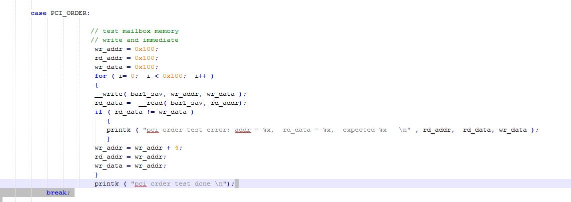
- Mark as New
- Bookmark
- Subscribe
- Mute
- Subscribe to RSS Feed
- Permalink
- Report Inappropriate Content
More ... I now have PCI_ORDER_PARK as below ... works fine prior to running NIOS II code ... after running NIOS II code , somehow I suspect the Avalon MM interconnect state changes and I get a the write data returned
from the constant IMEM location 0x10100 after the 8th PCIe write ( see error report image which is confirmed by the PCIe logic analyzer data probing the Gen1 X1 link ) The clue here may be that the write data is offset by 8 and I am wondering if the Avalon MM interconnect has an 8 deep FIFO somewhere ...I have seen it mentioned somewhere. How to fix : 1. reverse engineer the Avalon MM interconnect to see how the reads can pass writes for the BAR1 PCIe Hard IP Avalon MM master. 2. add SignalTap to the BAR1 Avalon MM master port to see what is happening. 3. investigate Hard IP to see if the BAR1 Avalon MM master port has the wrong settings. 4. try to determine why this failure only occurs after running NIOS II ... I will try just a "Hello from NIOS" message . I also see this on Cyclone , but it is worse I believe and the Cyclone is running NIOS out of the SSRAM on board. 5. investigate if the IMEM i'm using as a mailbod between NIOS and the Host ( RC ) needs to be dual ported. case PCI_ORDER_PARK: // test mailbox memory // write and immediate single location wr_addr = 0x10100; rd_addr = 0x10100; wr_data = 0x100; for ( i= 0; i < 0x100; i++ ) { __write( bar1_sav, wr_addr, wr_data ); rd_data = __read( bar1_sav, rd_addr); if ( rd_data != wr_data ) { printk ( "pci order test error: addr = %x, rd_data = %x, expected %x \n" , rd_addr, rd_data, wr_data ); } wr_data++; } printk ( "pci order park test done \n"); break;
- Mark as New
- Bookmark
- Subscribe
- Mute
- Subscribe to RSS Feed
- Permalink
- Report Inappropriate Content
Try signaltap on the internal memory.
Make sure the nios data cache isn't (somehow) causing grief. You probably want to tightly couple the internal memory to the nios and dual port it to the avalon bus and hence the PCIe slave.- Mark as New
- Bookmark
- Subscribe
- Mute
- Subscribe to RSS Feed
- Permalink
- Report Inappropriate Content
Thanks DSL,
I made the IMEM mailbox ,which is the shared memory between the NIOS II and the PCIe BAR1 ( read host RC system ), dual_ported.... that is BAR1 -> port 0 and NIOS data -> port 1. Things improved but not fixed ... now the tests pass from the RC prior to NIOS II code running , same as before . With NIOS II code running I now have a 2 cycle offset rather than 8 cycle offset between write data from RC and the read data changing. That is after NIOS prints "Hello world" and returns. With NIOS application running , I see a 4 cycle offset ... so improved but not passing with NIOS yet. I examined the RTL and can't see where in the interconnect there are any FIFO's so it could be some kind of 2:1 arbiter for writes , holding writes off.- Mark as New
- Bookmark
- Subscribe
- Mute
- Subscribe to RSS Feed
- Permalink
- Report Inappropriate Content
Hi Bob,
I'm trying to create a PCIe endpoint on my Arria V starter board and trying to use the altpcie_demo_64.exe from the altera ref design to enumerate and do read/write to the fpga endpoint, but I'm getting all kinds of problems from the altpcie_demo not working...to the blue screen followed by my pc crashing. Can you assist since you've gotten the endpt working on your Arria V? Here's some of the things I'm doing: 1) following the Arria V Hard IP PCI express users guide (v.13.1 - Ch 3) I created the PCIe endpt and instantiated it making sure that I mapped to the correct fpga pins for the hard pcie IP. 2) Before, configuring the fpga I run the altpcie_demo_64 and the gui reports 78 devices. I also checked the device manager and only see the Jungo driver installed. 3) I program the fpga and then run the altpcie which reports 79 devices with one of the devices having the correct PCIe device and vendor ID - so this kinda tells me the PC has enumerated the fpga, right? However, the gui is greyed out so I can't do any read or write transactions to the fpga. Also, I noticed that the device manager has detected the Arria V dev kit - so that's good. However, sometimes I get the msg that the device doesn't have enough memory when I look at the devkit in the pc's device manager. Does this make any sense???? Sometimes it says the driver for the kit is working fine. Did you use the same Arria V starter board and did you use the altpcie_demo_64 too? I'd appreciate it a lot if you could share your wisdom in getting me past this hurdle of getting actual traffic going between the pc and the fpga. Thanks, Peter- Mark as New
- Bookmark
- Subscribe
- Mute
- Subscribe to RSS Feed
- Permalink
- Report Inappropriate Content
Hi Peter,
From my experience, geetting the Arria V Starter Kit board going was a fair amount of work but it should not have been. I was on a Linux system and had to learn Linux device driver by taking various examples and comming up with something that worked. On the Windows environemnt I would think it should be easier since with the Juno driver. I'm not sure about the 79 devices unless they actually exist. I did some work on a PC and found it useful using some of the existing tools to enumerate the slots after POST /BIOS which will say that your card has trained and is seen in the slot ... I had some trouble with various slots even at Gen1 due to slot width. I did run the sample application doing DMA and it measures write / read performance ... I can check whatthat was. It would have been the sample DMA application. Let me try to digest your points and get back to you. Bob.- Mark as New
- Bookmark
- Subscribe
- Mute
- Subscribe to RSS Feed
- Permalink
- Report Inappropriate Content
I'm going to run simulation on this but I'm not sure if I will be able to repeat the hardware fails ... I may get some insight though.
On the weekend I checked the PCIe Hard IP in QSYS and noticed under "Avalon MM System Settings" the "Single DW completer" is not checked ... checking this takes out the burst count signals from the Avalon MM BAR masters. I can look at the Simulation to see what difference this will make but I expect, it constrains the Master to single DW transfers. It is hard to believe the interconnect can be loosely ordered ... but probing the PCIe BAR1 Avalon MM master will say if the ordering issue is in the PCIe Hard IP or in the Avalon MM interconnect. The other thing is that the write / read test runs fine from the RC prior to starting NIOS II in the Eclipse environment ... after that the test fails. Even if the NIOS II code is just a single printf or even just return(0), I still get the errors. I would like to go into the debugger and see if it fails prior to any instruction execution ie just sitting at the entry point. I have never been able to get the PCIe Compiler to edit the PCIe Hard IP megafunctions even if I edit the .tcl definition to make it editable ... does any one have any experience with that or do we just go with the PCIe Hard IP that comes delivered for each FPGA family. Thanks, Bob.- Mark as New
- Bookmark
- Subscribe
- Mute
- Subscribe to RSS Feed
- Permalink
- Report Inappropriate Content
Peter,
sorry I did not get back to this ... Here's some of the things I'm doing: 1) following the Arria V Hard IP PCI express users guide (v.13.1 - Ch 3) I created the PCIe endpt and instantiated it making sure that I mapped to the correct fpga pins for the hard pcie IP. 2) Before, configuring the fpga I run the altpcie_demo_64 and the gui reports 78 devices. I also checked the device manager and only see the Jungo driver installed. 3) I program the fpga and then run the altpcie which reports 79 devices with one of the devices having the correct PCIe device and vendor ID - so this kinda tells me the PC has enumerated the fpga, right? However, the gui is greyed out so I can't do any read or write transactions to the fpga. Also, I noticed that the device manager has detected the Arria V dev kit - so that's good. However, sometimes I get the msg that the device doesn't have enough memory when I look at the devkit in the pc's device manager. Does this make any sense???? Sometimes it says the driver for the kit is working fine. Let me go back to this ... I have a couple of Arria V Starter Kit Boards and do recall running that sample application. I remember the GUI would check the PCIe slots and fail if the required ID was not found then a menu would come up with DMA Write/ Read tests and some performance measurements. I have experienced problems with Linus where the memory allocated for PCIe endpoints is less that the FPGA is requesting and the device driver fails. I can't recall anything like that on Window ... we have HP desksides and there was a situation where slots were protected by BIOS setting to disable them and lock out the addition of new endpoints but you are obviously beyond that . I will see if I can get back to that altpcie_demo_64. Best Regards, Bob.- Mark as New
- Bookmark
- Subscribe
- Mute
- Subscribe to RSS Feed
- Permalink
- Report Inappropriate Content
I wonder if the PCIe to Avalon bridge (for PCIe slave cycles) actually has two separate Avalon master interfaces, one for reads and one for writes?
That might allow a read transfer to overtake a write one - even though the PCIe master shouldn't have requested the read until after it has seen the completion message for the write.- Mark as New
- Bookmark
- Subscribe
- Mute
- Subscribe to RSS Feed
- Permalink
- Report Inappropriate Content
DSL ,
Re your earlier post ... I have the minimum NIOS II out of the 3 configurations and don't believe it has a data cache. On the PCIe Hard IP core, the BAR1 Avalon MM master indicates a single Address , a Write data and a Read data port ... so .... to get two channels ie a write and a read channel, that would need to happen in the Avalon MM interconnect fabric. I deal with loosely ordered systems but would not the Avalon MM interconnect fabric to be loosley ordered. In my Linux device driver, because the target system is loosely ordered there are read and write barriers inserted at appropriate synchronization points.- Mark as New
- Bookmark
- Subscribe
- Mute
- Subscribe to RSS Feed
- Permalink
- Report Inappropriate Content
I'm half-remembering the diagrams for the (IIRC) avalon streaming interfaces to the PCIe block. I think you can use them instead of the Avalon master interface. I'm sure there are separate tx and rx streams (I might just be thinking of the fpga being a PCIe master).
If I'm remembering correctly then it is likely that the avalon master is built on top of that interface. In which case nothing on the fpga will actually enforce that a write finishes before a read to the same address - even though the actual PCIe cycles have to be ordered. Hmmm... I've just realised you are talking about very long delays between the write and read cycles - not ones that are back to back on the pcie bus.- Mark as New
- Bookmark
- Subscribe
- Mute
- Subscribe to RSS Feed
- Permalink
- Report Inappropriate Content
Hi Peter,
I have been snowed under and think I may need to go to a second shift ... anyhow I am trying tpo go back to when I had a Windows system and was running the sample application you mentioned.... It was roughly 12 months ago .. but I am recalling some of it. Did you use the same Arria V starter board and did you use the altpcie_demo_64 too? No ...I used the Stratix V card ... I can try the Arria V GX Starter Kit card tomorrow. I have access to a Microsoft machine ... I recall the GUI came up and searched for the DeviceID / VendorID and complained iif it was not found. I can't recall any crashes, but know it leverages the Juno Device Driver ... can you say if that is installed OK ? Let me try to run it on the Arria V card and get back to you. Bob- Mark as New
- Bookmark
- Subscribe
- Mute
- Subscribe to RSS Feed
- Permalink
- Report Inappropriate Content
--- Quote Start --- Hi Bob, I'm trying to create a PCIe endpoint on my Arria V starter board and trying to use the altpcie_demo_64.exe from the altera ref design to enumerate and do read/write to the fpga endpoint, but I'm getting all kinds of problems from the altpcie_demo not working...to the blue screen followed by my pc crashing. Can you assist since you've gotten the endpt working on your Arria V? Here's some of the things I'm doing: 1) following the Arria V Hard IP PCI express users guide (v.13.1 - Ch 3) I created the PCIe endpt and instantiated it making sure that I mapped to the correct fpga pins for the hard pcie IP. 2) Before, configuring the fpga I run the altpcie_demo_64 and the gui reports 78 devices. I also checked the device manager and only see the Jungo driver installed. 3) I program the fpga and then run the altpcie which reports 79 devices with one of the devices having the correct PCIe device and vendor ID - so this kinda tells me the PC has enumerated the fpga, right? However, the gui is greyed out so I can't do any read or write transactions to the fpga. Also, I noticed that the device manager has detected the Arria V dev kit - so that's good. However, sometimes I get the msg that the device doesn't have enough memory when I look at the devkit in the pc's device manager. Does this make any sense???? Sometimes it says the driver for the kit is working fine. Did you use the same Arria V starter board and did you use the altpcie_demo_64 too? I'd appreciate it a lot if you could share your wisdom in getting me past this hurdle of getting actual traffic going between the pc and the fpga. Thanks, Peter --- Quote End --- Peter, are you saying you developed the FPGA code yourself ... 1) following the Arria V Hard IP PCI express users guide (v.13.1 - Ch 3) I created the PCIe endpt and instantiated it making sure that I mapped to the correct fpga pins for the hard pcie IP. And didn't use the sample HW configuration ...? I can't see a Arria V design when I look at the altpci demo designs. I see a Arria II design. Let me try to down load the Arria II design ... If you did design up an example from the user guide ... how would you know where to map the SG DMA registers to work in concert with the device driver that comes with the example .. or am I missing something ? I will try to download the .zip exaample for Arria II and see what it contains. Best Regards, Bob.
- Mark as New
- Bookmark
- Subscribe
- Mute
- Subscribe to RSS Feed
- Permalink
- Report Inappropriate Content
All this gets resolved if the RC and the EP card are reset each time I believe.
I don't have root cause but am monitoring it. It is possibly in emulation to reset the RC and maybe not all the EP state. I think the PCIe slot reset propagates to the Avalon MM fabric and internal IP but need to check. So I believe this is related to resetting the RC without a corresponding full reset of the FPGA EP.- Subscribe to RSS Feed
- Mark Topic as New
- Mark Topic as Read
- Float this Topic for Current User
- Bookmark
- Subscribe
- Printer Friendly Page