- Mark as New
- Bookmark
- Subscribe
- Mute
- Subscribe to RSS Feed
- Permalink
- Report Inappropriate Content
Hello,
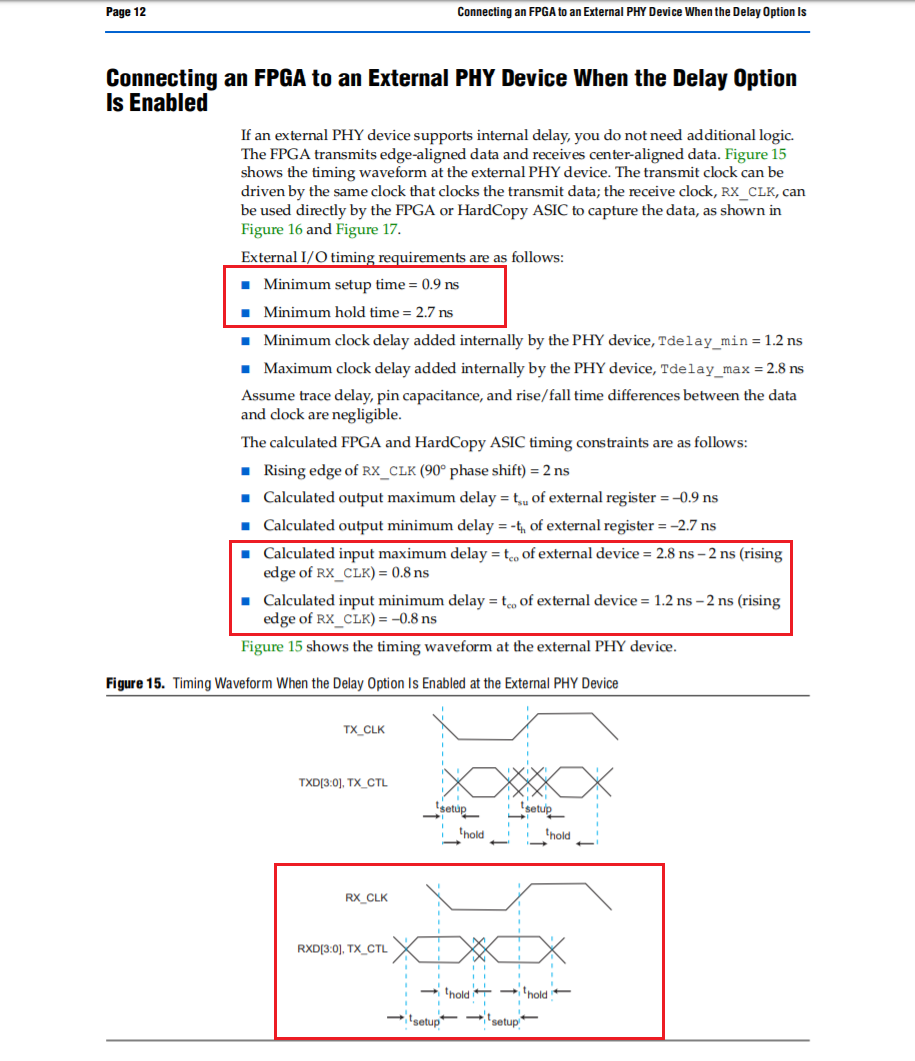
In page 12 of this document (Example 1):
https://www.intel.com/content/dam/www/programmable/us/en/pdfs/literature/an/an477.pdf
The example lists:
Minimum Setup time = 0.9 ns
Minimum hold time = 2.7 ns
Based on this - the example calculates the Max and Min input delays as follows :
Calculated input maximum delay = tco of external device = 2.8 ns – 2 ns (rising edge of RX_CLK) = 0.8 ns
Calculated input minimum delay = tco of external device = 1.2 ns – 2 ns (rising edge of RX_CLK) = –0.8 ns
However,
If we follow Intel's presentation about constraining source synchronous DDR interfaces (Example 2) the calculation will yeild a different result:
tui = 8.0 , Tsu = 0.9 , Th = 2.7
Calculated input maximum delay = tui / 2 - Tsu = 8 / 2 - 0.9 = 3.1 nS
Calculated input minimum delay = Th - tui / 2 = 2.7 - ( 8 / 2 ) = -1.3 nS
Am I getting something wrong or is there an error in one of the examples ?
Link Copied
- Mark as New
- Bookmark
- Subscribe
- Mute
- Subscribe to RSS Feed
- Permalink
- Report Inappropriate Content
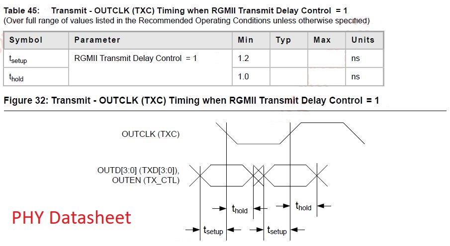
The setup and hold you are referencing (0.9 and 2.7) do not refer to the setup and hold requirements at the input of the FPGA. It appears from the document they refer to the requirements of the downstream device on the transmit side. See the SDC code on page 14 for the output (transmit) side. So the formula you are referencing is incorrect for the input. The correct formulas are on slide 3.5 as shown in the training table of contents there:
input delay max = data trace max - clock trace min + tcomax
input delay min = data trace min - clock trace max + tcomin
The app note appears to be ignoring trace delay differences (this is typical; clock and data trace usually are matched so they cancel each other out) and calculating just tcomax and tcomin based on:
tcomax = tcomax(data) - tcomin(clock) = 2.8 - 2 = 0.8
tcomin = tcomin(data) - tcomax(clock) = 1.2 - 2 = -0.8
It's a little strange for me to see the delay due to the phase shift (2 ns) used as the tco for the clock path, but it does make sense as slide 3.5 says to get a tco with respect to the PHY's input clock instead of its output clock, and the code on page 15 indicates that the input delay is relative to the rising or falling edge.
Hope this helps.
#iwork4intel
- Mark as New
- Bookmark
- Subscribe
- Mute
- Subscribe to RSS Feed
- Permalink
- Report Inappropriate Content
- Mark as New
- Bookmark
- Subscribe
- Mute
- Subscribe to RSS Feed
- Permalink
- Report Inappropriate Content
Hi Sir,
Seems like you are facing additional issue on timing. Currently we serve forum case per area basis. For new issue, appreciated if you can open a new thread to get the support from Intel experts. Thank you.
- Subscribe to RSS Feed
- Mark Topic as New
- Mark Topic as Read
- Float this Topic for Current User
- Bookmark
- Subscribe
- Printer Friendly Page