- Mark as New
- Bookmark
- Subscribe
- Mute
- Subscribe to RSS Feed
- Permalink
- Report Inappropriate Content
For example, I don't want to use a LAB named "LABCELL_X66_Y55_N6".
How do I let Quartus Prime know this, and avoid using this LAB in compiling my design?
Thank you.
Link Copied
- Mark as New
- Bookmark
- Subscribe
- Mute
- Subscribe to RSS Feed
- Permalink
- Report Inappropriate Content
I'm not sure why you don't want to use a particular resource, but you can force logic into resources you do want to use with Logic Lock regions in the Chip Planner. Draw shapes (rectangular by default; merge them together to make non-rectangular shapes) and assign logic from your design to a region. Then the Fitter is forced to place the logic in that region.
Be aware that if you have a very full design, this could cause no-fit or timing issues due to you forcing logic into specific locations, away from where the Fitter would prefer to place it.
- Mark as New
- Bookmark
- Subscribe
- Mute
- Subscribe to RSS Feed
- Permalink
- Report Inappropriate Content
Hi sstrell:
Thanks for your reply, but it's not the answer what I approach for.
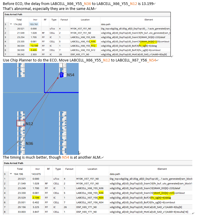
I want to forbid Quartus Prime to use a particular resource, because I find some particular LAB delay is 10x larger than a normal LAB in Timing Analyzer. After I use chip planner for post-netlist ECO to change the LAB resource to a adjacent LAB, the problem is solved. So, I think the 10x delay LAB may be something wrong.
I appreciate it if you could kindly provide a solution for my request.
- Mark as New
- Bookmark
- Subscribe
- Mute
- Subscribe to RSS Feed
- Permalink
- Report Inappropriate Content
I don't understand how a particular LAB could be slower than any other. They are identical. Can you share your .sdc and the timing report where you're seeing this? There is some reason why the Fitter is selecting this LAB for you (super full design perhaps?) and causing the issue. The extra delay may be getting a signal to a particular physical location, not the physical resource itself. If that's the case, you need to figure out why the Fitter is doing this.
The ECO fixes it, but it might be useful going forward to understand the cause of the issue.
- Mark as New
- Bookmark
- Subscribe
- Mute
- Subscribe to RSS Feed
- Permalink
- Report Inappropriate Content
Hi Sstrell:
I don't understand that either, but it happens.
I provide the Chip Planner layout and Timing report here.
The utilization of my design is 27%, and I think it's not an issue for FPGA fitter.
BTW, if you know how to avoid using a specific LAB in Quartus Prime, please tell me how. Thank you.
- Mark as New
- Bookmark
- Subscribe
- Mute
- Subscribe to RSS Feed
- Permalink
- Report Inappropriate Content
As I suspected, IC is interconnect delay where you're seeing the problem, not LAB (cell) delay. For some reason, the Fitter is using long routing wires which doesn't make sense as you say since they're in the same LAB.
When you run Report Timing in the Timing Analyzer, turn on the Show Routing option. That breaks down IC delay into RE (routing element) delay.
There must be some physical reason why the Fitter is doing this. Again, it would also be useful to see your timing constraints, at least what speed you're trying to run this at.
- Mark as New
- Bookmark
- Subscribe
- Mute
- Subscribe to RSS Feed
- Permalink
- Report Inappropriate Content
Hi Sstrell:
Thanks you.
Your suspicion is right, and the large IC delay is caused by lots of RE delay.
Though the data path is within the same LAB cell, Quartus II still deliver this long long routing path.
Do you have any idea why Quartus II does it?
My design is a simple image processor. The PLL clock in is 64MHz, and my design runs at 32MHz.
Utilization = 27% on Cyclone V-E FPGA.
- Mark as New
- Bookmark
- Subscribe
- Mute
- Subscribe to RSS Feed
- Permalink
- Report Inappropriate Content
Hi Sheng,
Any other concern on this?
- Mark as New
- Bookmark
- Subscribe
- Mute
- Subscribe to RSS Feed
- Permalink
- Report Inappropriate Content
Yes, the data path is within the same LAB cell, Quartus II still deliver a long routing path. (10x larger than other path)
Is it a normal situation for a low-speed (32MHz) and low-utilization (27%) design?
Could you give me some opinions for explaining why Quartus II did this?
- Mark as New
- Bookmark
- Subscribe
- Mute
- Subscribe to RSS Feed
- Permalink
- Report Inappropriate Content
Can you show the timing report details for the long path (including the routing and logic elements involved)? The HDL for that part of the design? RTL or Tech Map Viewer schematic?
Do you have any relevant assignments in the Assignment Editor that might be forcing this?
More info is needed to figure out what is going on here.
- Mark as New
- Bookmark
- Subscribe
- Mute
- Subscribe to RSS Feed
- Permalink
- Report Inappropriate Content
Hi Sheng,
Any update?
- Subscribe to RSS Feed
- Mark Topic as New
- Mark Topic as Read
- Float this Topic for Current User
- Bookmark
- Subscribe
- Printer Friendly Page