- Mark as New
- Bookmark
- Subscribe
- Mute
- Subscribe to RSS Feed
- Permalink
- Report Inappropriate Content
I include the sclr control in my code, but it will not connect to the sclr pin of altera_syncram. I tried to instantiate a ram ip, and enable the sclr, I can see that my sclr will connect to the sclr pin. Is there a way to add the sclr in the vhdl code? The following is the code:
process(l_clk)
begin
if rising_edge(l_clk) then
if l_wr_en = '1' then
ram(l_addr) <= l_wr_data;
end if;
if srst = '1' then
r_rd_data_i <= (others => '-');
elsif r_rd_en then
r_rd_data_i <= ram((r_addr);
else
r_rd_data_i <= r_rd_data_i;
end if;
r_rd_data <= r_rd_data_i;
end if;
end process;
Link Copied
- Mark as New
- Bookmark
- Subscribe
- Mute
- Subscribe to RSS Feed
- Permalink
- Report Inappropriate Content
Try changing (others => '-') to (others => '0'). Alternatively, are you sure you want the reset on r_rd_data_i and not r_rd_data?
- Mark as New
- Bookmark
- Subscribe
- Mute
- Subscribe to RSS Feed
- Permalink
- Report Inappropriate Content
Hi,
"but it will not connect to the sclr pin of altera_syncram" -- Can you provide the complete code or project file(Project -> Archive project)?
"Is there a way to add the sclr in the vhdl code? " -- what error/simulation result you observed?
Regards,
Vicky
- Mark as New
- Bookmark
- Subscribe
- Mute
- Subscribe to RSS Feed
- Permalink
- Report Inappropriate Content
Hi
Thank you very much for your supply.
I am doing some research on how to use alter_syncram of Stratix 10. We are moving from Arria 10 to stratix 10. Before, we use ip editor to instantiate altersyncram of Arria 10 by setting parameters, such as:
altsyncram_inst : altsyncram
generic map (
init_file => init_file,
address_aclr_b => "NONE",
address_reg_b => "CLOCK1",
clock_enable_input_a => CLOCK_ENABLE_IO_AB,
clock_enable_input_b => CLOCK_ENABLE_IO_AB,
clock_enable_output_b => CLOCK_ENABLE_IO_AB,
intended_device_family => getAlteraDeviceName(DEVICE),
lpm_type => "altsyncram",
numwords_a => 2**l_a_width,
numwords_b => 2**R_A_WIDTH_EFFECTIVE,
operation_mode => "DUAL_PORT",
outdata_aclr_b => "CLEAR1",
outdata_reg_b => "CLOCK1",
power_up_uninitialized => "FALSE",
ram_block_type => ram_type,
rdcontrol_reg_b => "CLOCK1",
widthad_a => l_a_width,
widthad_b => R_A_WIDTH_EFFECTIVE,
width_a => l_d_width,
width_b => R_D_WIDTH_EFFECTIVE,
width_byteena_a => 1
)
port map (
-- asynch reset
aclr1 => arst,
-- left port clock domain
clock0 => l_clk,
wren_a => l_wr_en,
address_a => l_addr,
data_a => l_wr_data,
-- right port clock domain
clock1 => r_clk,
rden_b => r_rd_en,
address_b => r_addr,
q_b => r_rd_data
);
This method is device dependent, because the parameter of "intended_device_family". We found the Qaurtus will implement a ram if we define a 2-D array in our VHDL code. I feel this method is more flexible and device independent, which is easier to move from one device to another. Now we are doing test to see the difference. The following is some problems we met.
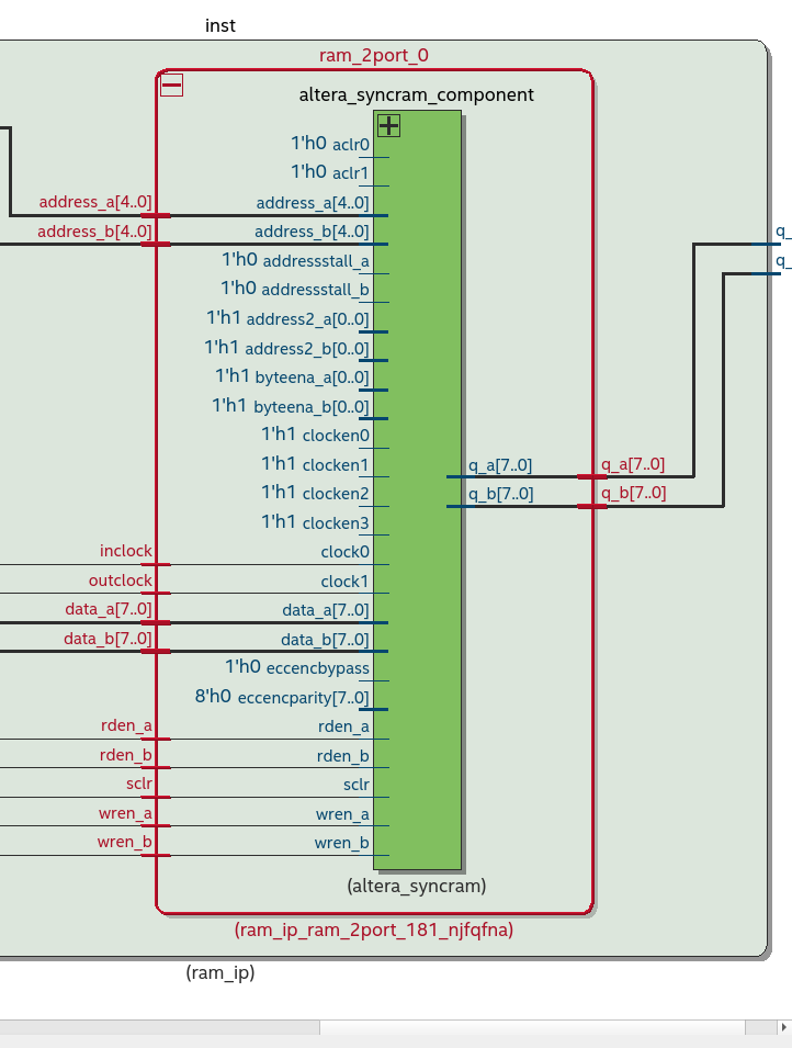
(1) By using ip editor, we can see the "sclr" signal can be enabled by checking the corresponding setting in ip editor, and the external control is connected to the slcr pin of RAM:
The following is the VHDL code with sclr signal, which is modified based on the template from Quartus prime pro:
-- Quartus Prime VHDL Template
-- True Dual-Port RAM with dual clocks
--
-- This style of RAM cannot be used on Stratix 10,
-- which does not support True Dual Port RAM with dual clocks
library ieee;
use ieee.std_logic_1164.all;
use IEEE.numeric_std.all;
entity dp_dc_ram is
generic
(
DATA_WIDTH : natural := 8;
ADDR_WIDTH : natural := 6
);
port
(
l_clk : in std_logic;
r_clk : in std_logic;
l_addr : in natural range 0 to 2**ADDR_WIDTH - 1;
r_addr : in natural range 0 to 2**ADDR_WIDTH - 1;
l_wr_data : in std_logic_vector((DATA_WIDTH-1) downto 0);
r_wr_data : in std_logic_vector((DATA_WIDTH-1) downto 0);
l_wr_en : in std_logic := '1';
r_wr_en : in std_logic := '1';
l_rd_data : out std_logic_vector((DATA_WIDTH -1) downto 0);
r_rd_data : out std_logic_vector((DATA_WIDTH -1) downto 0);
sclr : in std_logic;
l_rd_en : in std_logic;
r_rd_en : in std_logic
);
end dp_dc_ram;
architecture rtl of dp_dc_ram is
-- Build a 2-D array type for the RAM
subtype word_t is std_logic_vector((DATA_WIDTH-1) downto 0);
type memory_t is array(2**ADDR_WIDTH-1 downto 0) of word_t;
-- Declare the RAM
shared variable d_ram : memory_t;
signal l_rd_data_i : std_logic_vector((DATA_WIDTH -1) downto 0);
signal r_rd_data_i : std_logic_vector((DATA_WIDTH -1) downto 0);
begin
-- Port A
process(l_clk)
begin
if rising_edge(l_clk) then
if l_wr_en = '1' then
d_ram(l_addr) := l_wr_data;
end if;
end if;
end process;
process (l_clk)
begin
if rising_edge(l_clk) then
-- On a read during a write to the same address, the read will
-- return the OLD data at the address
if sclr = '1' then
l_rd_data_i <= (others => '0');
elsif l_rd_en then
l_rd_data_i <= d_ram(l_addr);
else
l_rd_data_i <= l_rd_data_i;
end if;
l_rd_data <= l_rd_data_i;
end if;
end process;
-- Read and wirte operation on right port.
process(r_clk)
begin
if rising_edge(r_clk) then
if r_wr_en = '1' then
d_ram(r_addr) := r_wr_data;
end if;
end if;
end process;
process(r_clk)
begin
if rising_edge(r_clk) then
-- On a read during a write to the same address, the read will
-- return the OLD data at the address
if sclr = '1' then
r_rd_data_i <= (others => '0');
elsif r_rd_en then
r_rd_data_i <= d_ram(r_addr);
else
r_rd_data_i <= r_rd_data_i;
end if;
r_rd_data <= r_rd_data_i;
end if;
end process;
end rtl;
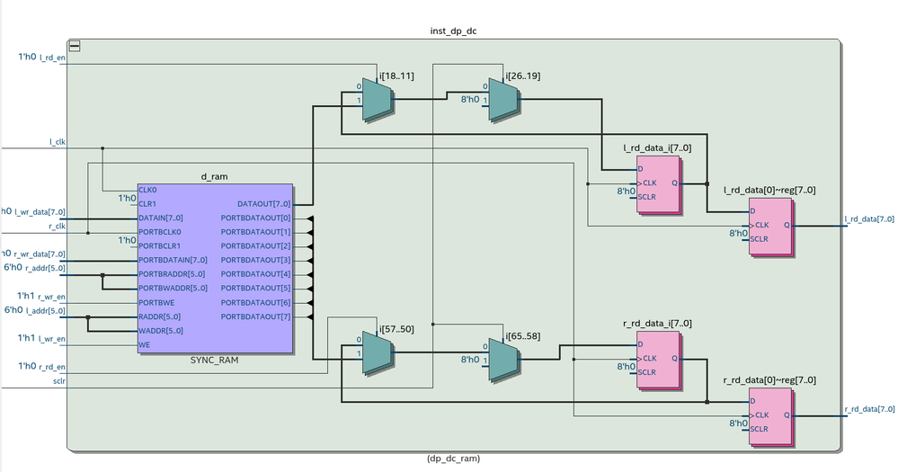
The rtl circuit is:
Comparing the two rtl circuits, you can the sclr doesn't connect the sclr pin of ram in the later one. And the same situation happens to the DFF as well. Is there anything wrong from my code, or should there be any parameters to enable the sclr of ram?
(2) The other question is about the implementation of true dual port dual clock ram. From ip editor, it only supports two read/write ports with input/output clock, which means all input signal are registered by clock0, and all output signals are registered by clock1. In this case, my understanding is that all signals except q_a and q_b are using clock0, is that correct? We need to use a two port ram with independent clocks: port A is driven by clock0, ad port B is driven by clock1. It seems there is no problem if we use vhdl to implement it (please see the above code and rtl circuit, the r_clk is connected to portB clk), but can not with ip editor. Is there any limitation to use true dual ports with independent clocks?
Thank you very much!
Xin
- Mark as New
- Bookmark
- Subscribe
- Mute
- Subscribe to RSS Feed
- Permalink
- Report Inappropriate Content
Hi Xin,
1. The code provided over here, having multiple errors,please provide code which has been compiled without error if possible provide project file(.qar)(Project menu-> Archive Project)
2. true dual port dual clock ram. From ip editor, it only supports two read/write ports with input/output clock, which means all input signal are registered by clock0, and all output signals are registered by clock1. In this case, my understanding is that all signals except q_a and q_b are using clock0, is that correct? -- --here output clock will control only the data output registers & rest of the registers are controlled by input clock.
3. We need to use a two port ram with independent clocks: port A is driven by clock0, ad port B is driven by clock1. --- You have to use Read/Write Clock Mode.
4. Is there any limitation to use true dual ports with independent clocks? --- Yes,this can be done using Emulate TDP dual clock mode & this option is available only if you select With two read/write ports and Customize clocks for A and B ports clocking method.
Refer the below user guide for more details,
Regards,
Vicky
- Mark as New
- Bookmark
- Subscribe
- Mute
- Subscribe to RSS Feed
- Permalink
- Report Inappropriate Content
- Mark as New
- Bookmark
- Subscribe
- Mute
- Subscribe to RSS Feed
- Permalink
- Report Inappropriate Content
- Mark as New
- Bookmark
- Subscribe
- Mute
- Subscribe to RSS Feed
- Permalink
- Report Inappropriate Content
Hi Xin,
As I suggested in previous post , If you want to use Emulate TDP in your project then you have to fulfill the requirement as mentioned in user guide.
Another way is you can generate the HDL(*.vh,*v) file for Emulate TDP & then modify that HDL file as per your requirement, eventually you should verify it by writing testbench for that.
Regards,
Vicky
- Subscribe to RSS Feed
- Mark Topic as New
- Mark Topic as Read
- Float this Topic for Current User
- Bookmark
- Subscribe
- Printer Friendly Page

