- Marquer comme nouveau
- Marquer
- S'abonner
- Sourdine
- S'abonner au fil RSS
- Surligner
- Imprimer
- Signaler un contenu inapproprié
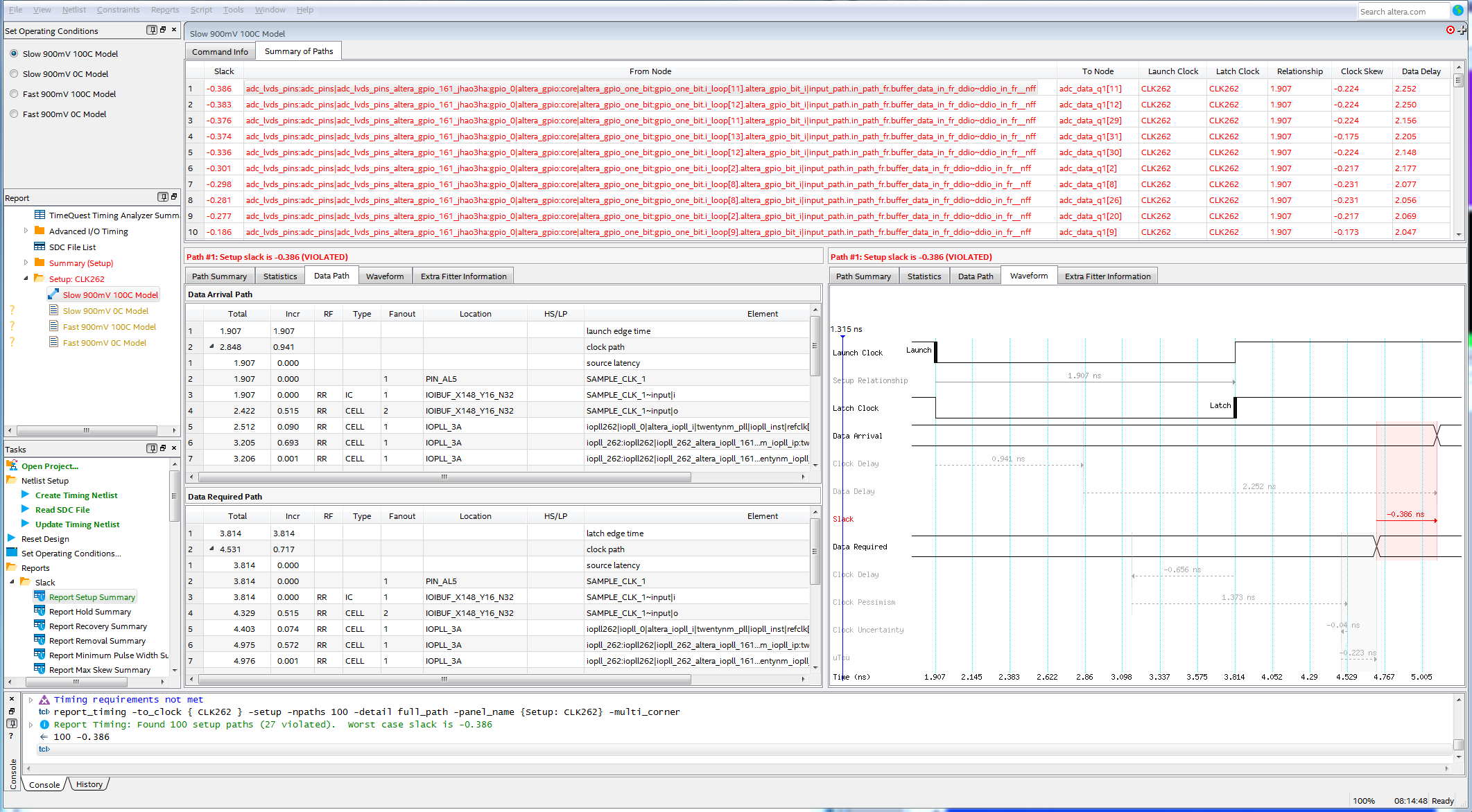
I have a setup violation at the register after the input register. The input register is constrained as described in AN433.
set_input_delay -add_delay -clock virt_adc_clk -min -0.6             [get_ports {ADC_DATA[*]}]
set_input_delay -add_delay -clock virt_adc_clk -min -0.6 -clock_fall [get_ports {ADC_DATA[*]}]

set_input_delay -add_delay -clock virt_adc_clk -max  0.6             [get_ports {ADC_DATA[*]}]
set_input_delay -add_delay -clock virt_adc_clk -max  0.6 -clock_fall [get_ports {ADC_DATA[*]}]

set_false_path -setup -fall_from [get_clocks virt_adc_clk] -rise_to \
[get_clocks CLK262]
set_false_path -setup -rise_from [get_clocks virt_adc_clk] -fall_to \
[get_clocks CLK262]
set_false_path -hold -rise_from [get_clocks virt_adc_clk] -rise_to \
[get_clocks CLK262]
set_false_path -hold -fall_from [get_clocks virt_adc_clk] -fall_to \
[get_clocks CLK262]
But now i have the violation after the input register, as you can see in the picture from Timequest.
Do I miss something?
Lien copié
- Marquer comme nouveau
- Marquer
- S'abonner
- Sourdine
- S'abonner au fil RSS
- Surligner
- Imprimer
- Signaler un contenu inapproprié
Can you show your clock constraints from the SDC?
#iwork4intel
- Marquer comme nouveau
- Marquer
- S'abonner
- Sourdine
- S'abonner au fil RSS
- Surligner
- Imprimer
- Signaler un contenu inapproprié
Thank you for your answer.
I tried this:
create_clock -period "262.144 MHz" -name  virt_adc_clk
create_clock -period "262.144 MHz" -name  {SAMPLE_CLK_1} {SAMPLE_CLK_1}

create_generated_clock 	-name {CLK262} \
								-source [get_ports {SAMPLE_CLK_1}] \
								-divide_by 1 \
								-multiply_by 1 \
								-phase 90 \
   							-duty_cycle 50.00 { iopll262|iopll_0|altera_iopll_i|twentynm_pll|iopll_inst|outclk[0] }

derive_pll_clocks -create_base_clocks
and also this without phase shift:
create_clock -period "262.144 MHz" -name  virt_adc_clk
create_clock -period "262.144 MHz" -name  {SAMPLE_CLK_1} {SAMPLE_CLK_1}

create_generated_clock 	-name {CLK262} \
								-source [get_ports {SAMPLE_CLK_1}] \
								-divide_by 1 \
								-multiply_by 1 \
   							-duty_cycle 50.00 { iopll262|iopll_0|altera_iopll_i|twentynm_pll|iopll_inst|outclk[0] }

derive_pll_clocks -create_base_clocks
The violations are the same. For the appplication is no difference because we use the ADC AD9652 and we adjust the DCO by starting the system.
- Marquer comme nouveau
- Marquer
- S'abonner
- Sourdine
- S'abonner au fil RSS
- Surligner
- Imprimer
- Signaler un contenu inapproprié
Get rid of the generated clock constraint. derive_pll_clocks does that for you. Also, is this edge-aligned or center-aligned? Instead of using -create_base_clocks, you need to have a create_clock constraint that properly defines the relationship between the virtual clock and the clock coming into the FPGA depending on that alignment using the -waveform option.
#iwork4intel
- Marquer comme nouveau
- Marquer
- S'abonner
- Sourdine
- S'abonner au fil RSS
- Surligner
- Imprimer
- Signaler un contenu inapproprié
This is edge-aligned. I changed to your recommendations and now Quartus compiles the design. This will takes some hours.
create_clock -period "262.144 MHz" -name  virt_adc_clk -waveform {0.0 1.907}
create_clock -period "262.144 MHz" -name  {SAMPLE_CLK_1} {SAMPLE_CLK_1} -waveform {0.0 1.907}

derive_pll_clocks -create_base_clocks

set_input_delay -add_delay -clock virt_adc_clk -min -0.6             [get_ports {ADC_DATA[*]}]
set_input_delay -add_delay -clock virt_adc_clk -min -0.6 -clock_fall [get_ports {ADC_DATA[*]}]

set_input_delay -add_delay -clock virt_adc_clk -max  0.6             [get_ports {ADC_DATA[*]}]
set_input_delay -add_delay -clock virt_adc_clk -max  0.6 -clock_fall [get_ports {ADC_DATA[*]}]

set_false_path -setup -fall_from [get_clocks virt_adc_clk] -rise_to \
[get_clocks iopll262|iopll_0|adc_clk]
set_false_path -setup -rise_from [get_clocks virt_adc_clk] -fall_to \
[get_clocks iopll262|iopll_0|adc_clk]
set_false_path -hold -rise_from [get_clocks virt_adc_clk] -rise_to \
[get_clocks iopll262|iopll_0|adc_clk]
set_false_path -hold -fall_from [get_clocks virt_adc_clk] -fall_to \
[get_clocks iopll262|iopll_0|adc_clk]
Should I delete the -create_base_clocks? I thought I need it forc other PPLs.
- Marquer comme nouveau
- Marquer
- S'abonner
- Sourdine
- S'abonner au fil RSS
- Surligner
- Imprimer
- Signaler un contenu inapproprié
- Marquer comme nouveau
- Marquer
- S'abonner
- Sourdine
- S'abonner au fil RSS
- Surligner
- Imprimer
- Signaler un contenu inapproprié
Yes, get rid of create_base_clocks unless with "I thought I need it forc other PPLs." you mean that you have other PLLs in your design that are sourced from other input reference clocks. I'd still manually create all the base clocks, though.
#iwork4intel
- Marquer comme nouveau
- Marquer
- S'abonner
- Sourdine
- S'abonner au fil RSS
- Surligner
- Imprimer
- Signaler un contenu inapproprié
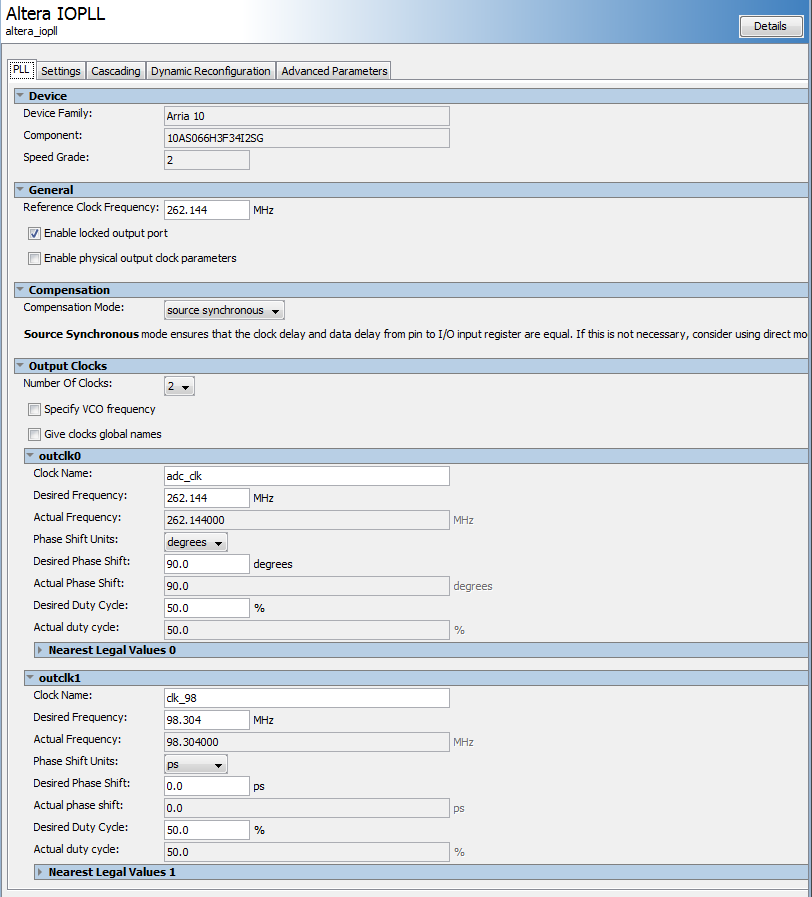
I think I made a mistake with the settings of the PLL. I used -90° instead of 90° phase shift. With this and the assignments:
set_false_path -setup -fall_from [get_clocks virt_adc_clk] -rise_to \
[get_clocks iopll262|iopll_0|adc_clk]
set_false_path -setup -rise_from [get_clocks virt_adc_clk] -fall_to \
[get_clocks iopll262|iopll_0|adc_clk]
set_false_path -hold -rise_from [get_clocks virt_adc_clk] -rise_to \
[get_clocks iopll262|iopll_0|adc_clk]
set_false_path -hold -fall_from [get_clocks virt_adc_clk] -fall_to \
[get_clocks iopll262|iopll_0|adc_clk]
I cuttet the wrong transfers.
Now with 90° pase shift I also get slacks at the input registers.
I could not find the maximum achievable frequency for the LVDS DDIO GPIO with an Arria 10 10AS066H3F34I2SG. Where can I find it?
Please find the test design in the attachment.
Thank you for your help!
- Marquer comme nouveau
- Marquer
- S'abonner
- Sourdine
- S'abonner au fil RSS
- Surligner
- Imprimer
- Signaler un contenu inapproprié
Hi,
There is no qpf and qsf files in the QAR attached. Could you archive again? May I know what version of the software you are using?
Thanks.
- Marquer comme nouveau
- Marquer
- S'abonner
- Sourdine
- S'abonner au fil RSS
- Surligner
- Imprimer
- Signaler un contenu inapproprié
Hi,
because of this issue we still use Quartus Prime 16.1.1 Build 200
https://www.intel.com/content/altera-www/global/en_us/index/support/support-resources/knowledge-base/ip/2019/why-is-the-last-output-frame-of-the-intel--fft-ip-core-missing-e.html
I manually added the qpf and qsf to the archive.
Thank you for your help.
- Marquer comme nouveau
- Marquer
- S'abonner
- Sourdine
- S'abonner au fil RSS
- Surligner
- Imprimer
- Signaler un contenu inapproprié
- Marquer comme nouveau
- Marquer
- S'abonner
- Sourdine
- S'abonner au fil RSS
- Surligner
- Imprimer
- Signaler un contenu inapproprié
Hi,
I am still looking into this.Please allow me some time on this.
Thanks.
- Marquer comme nouveau
- Marquer
- S'abonner
- Sourdine
- S'abonner au fil RSS
- Surligner
- Imprimer
- Signaler un contenu inapproprié
Hi,
thank you for your message.
- Marquer comme nouveau
- Marquer
- S'abonner
- Sourdine
- S'abonner au fil RSS
- Surligner
- Imprimer
- Signaler un contenu inapproprié
Hi,
I checked in the Timing Analyzer. The register is located within the I/O. According to the user guide https://www.intel.com/content/dam/www/programmable/us/en/pdfs/literature/ug/ug_altera_gpio.pdf, you may set the delay elements manually in the Intel Quartus Prime settings file (.qsf).
Input Delay Element
set_intance_assignment –to <PIN> -name INPUT_DELAY_CHAIN <0..63>
Output Delay Element set_intance_assignment –to <PIN> -name OUTPUT_DELAY_CHAIN <0..15>
Output Enable Delay Element
set_intance_assignment –to <PIN> -name OE_DELAY_CHAIN <0..15>
You may try to set the max and min value and see if it helps the timing. If no, this is the maximum frequency you can achieve with the I/O standard you have set, 1.8V
Thanks.
- Marquer comme nouveau
- Marquer
- S'abonner
- Sourdine
- S'abonner au fil RSS
- Surligner
- Imprimer
- Signaler un contenu inapproprié
Hi,
I tried with Input Delay 0, 1 and 63.
With more delay the setup slack is higher. With Delay set to 1 the hold slack is positive.
I also tried with FAST_INPUT_REGISTER on. No difference.
I never got less than -0.962ns setup slack.
The data delay is 1.341ns. Is the the correct value for a register located within the I/O?
Thanks
- Marquer comme nouveau
- Marquer
- S'abonner
- Sourdine
- S'abonner au fil RSS
- Surligner
- Imprimer
- Signaler un contenu inapproprié
Hi,
I am sorry for the late reply as I was out of office for 5 days.
The I/O standard you are using is 1.8V. According to the User guide, https://www.intel.com/content/dam/www/programmable/us/en/pdfs/literature/hb/arria-10/a10_handbook.pdf, user has to use terminated I/O standards if the GPIO is operating at a frequency higher than 250 MHz. SSTL, HSTL, POD and HSUL I/O standards are terminated I/O standards.
Thanks.
- Marquer comme nouveau
- Marquer
- S'abonner
- Sourdine
- S'abonner au fil RSS
- Surligner
- Imprimer
- Signaler un contenu inapproprié
H,
I changed the I/O Standard to Differential 1.8V SSTL Class 1, but the negative slack is still there.
In the handbook Intel recommends to use PHYLite for source synchronous Interfaces with more than 200 Mbps.
I tried to set the parameters for this IP.
I set the Interface clock to 262.144MHz, clock rate of user logic: Full
If I do so, I cannot set the PLL reference clock to 262.144MHz. Just half of it, but I need to set this clock, because it is coming from the ADC.
I don't know why it is not possible. In the PHYLite User Guide
https://www.intel.com/content/www/us/en/programmable/documentation/bhc1410942178562.html#bhc1410941851660/en-us Table 3
the Max Core Clock Rate (Full) with Arria 10 Speed Grade -2 is 266MHz.
Do I miss something?
Thanks.
- Marquer comme nouveau
- Marquer
- S'abonner
- Sourdine
- S'abonner au fil RSS
- Surligner
- Imprimer
- Signaler un contenu inapproprié
Hi,
To update, I am still looking into this. Please allow me some time on this.
Thanks.
- Marquer comme nouveau
- Marquer
- S'abonner
- Sourdine
- S'abonner au fil RSS
- Surligner
- Imprimer
- Signaler un contenu inapproprié
Hi,
I checked with the team, you have to use Phy Lite for frequency above 200 MHz.
Thanks.
- Marquer comme nouveau
- Marquer
- S'abonner
- Sourdine
- S'abonner au fil RSS
- Surligner
- Imprimer
- Signaler un contenu inapproprié
Hi,
I tried Phy Lite but had problems with setting the correct frequencies as I wrote 19 days before.
The text was:
In the handbook Intel recommends to use PHYLite for source synchronous Interfaces with more than 200 Mbps.
I set the Interface clock to 262.144MHz, clock rate of user logic: Full
If I do so, I cannot set the PLL reference clock to 262.144MHz. Just half of it, but I need to set this clock, because it is coming from the ADC.
I don't know why it is not possible. In the PHYLite User Guide
https://www.intel.com/content/www/us/en/programmable/documentation/bhc1410942178562.html#bhc1410941851660/en-us Table 3
the Max Core Clock Rate (Full) with Arria 10 Speed Grade -2 is 266MHz.
Thanks.
- Marquer comme nouveau
- Marquer
- S'abonner
- Sourdine
- S'abonner au fil RSS
- Surligner
- Imprimer
- Signaler un contenu inapproprié
Hi,
Can you provide the design.qar that is using the PhyLite so that I can look into it?
Thanks.
- S'abonner au fil RSS
- Marquer le sujet comme nouveau
- Marquer le sujet comme lu
- Placer ce Sujet en tête de liste pour l'utilisateur actuel
- Marquer
- S'abonner
- Page imprimable