- Mark as New
- Bookmark
- Subscribe
- Mute
- Subscribe to RSS Feed
- Permalink
- Report Inappropriate Content
Link Copied
- Mark as New
- Bookmark
- Subscribe
- Mute
- Subscribe to RSS Feed
- Permalink
- Report Inappropriate Content
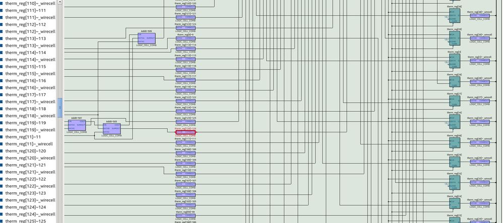
It would be helpful to see the RTL code for this to figure it out. You can right-click the highlighted cell and select to locate back to the code. Also, is this the RTL Viewer or the Technology Map Viewer (guessing Tech Map Viewer but just want to verify)? And what exactly is that highlighted cell connecting to? It goes off the edge of the screenshot.
#iwork4intel
- Mark as New
- Bookmark
- Subscribe
- Mute
- Subscribe to RSS Feed
- Permalink
- Report Inappropriate Content
The graphic view I show is from technology map viewer. The downstream connection from the LE buffer is a D input to a FF.
I'm trying to build a time to digital converter and need to place the FF in the same LE as the adder cells. The VHDL is very simple (shown below). The instantiation of this module simply makes the 'a' operand all '0's (128 of them, i.e., TDC_ELEMENTS_NB is 128) and the 'b' operand all '1's except for the low order bit which is driven with a rising transition from a launch register.. The entire 128-bits of the adder are placed in a logic logic region. I seem to find that this 'LE buffer insertion' happens quite often -- all through the design actually. Could it be related to the clocking scheme I'm using? The Clk shown below is actually driven from a FF in my design - I've made the output of the FF a global clock signal in the assignment editor.
entity TDC is
port (
Clk: in std_logic;
RESET: in std_logic;
a: in std_logic_vector(TDC_ELEMENTS_NB-1 downto 0);
b: in std_logic_vector(TDC_ELEMENTS_NB-1 downto 0);
TDC_therm_code: out std_logic_vector(TDC_ELEMENTS_NB-1 downto 0)
);
end entity;
architecture beh of TDC is
signal therm_next, therm_reg : signed (TDC_ELEMENTS_NB downto 0);
begin
process(Clk, RESET)
begin
if ( RESET = '1' ) then
therm_reg <= (others => '1');
elsif ( Clk'event and Clk = '1' ) then
therm_reg <= therm_next;
end if;
end process;
therm_next <= ('0' & signed(a)) + ('0' & signed(b));
TDC_therm_code <= std_logic_vector(therm_reg(TDC_ELEMENTS_NB-1 downto 0));
end beh;
- Mark as New
- Bookmark
- Subscribe
- Mute
- Subscribe to RSS Feed
- Permalink
- Report Inappropriate Content
Have you tried not using a Logic Lock region? Any reason why you need it (tight timing requirement perhaps)? Buffers are inserted for some more complex design flows (like partial reconfiguration) for Logic Lock regions to reserve locations for signals going in and out of the region. That could be the case here (I don't know what part of your design is encompassed by the Logic Lock region) though I don't recall seeing this if you are not using a more complex design flow. It can't hurt to try.
#iwork4intel
- Mark as New
- Bookmark
- Subscribe
- Mute
- Subscribe to RSS Feed
- Permalink
- Report Inappropriate Content
I can try it but the adder and the FFs (from the VHDL code) are in the logic lock region, and the buffers are inserted between the adder and FFs. Clearly the buffers are adding delay to these paths. Why are they being inserted? Are they put in to meet hold time constraints? I've tried several fitter options, e.g., set_global_assignment -name OPTIMIZE_HOLD_TIMING "IO PATHS AND MINIMUM TPD PATHS" (default is all paths) but nothing seems to work. I'm curious if there is a synthesis or fitter setting that would eliminate them. Alteratively, I could set a tight timing constraint on all of these paths (would be a lot of work) to try to force the tool to leave them out if you think that would be the best (or only) option.
- Mark as New
- Bookmark
- Subscribe
- Mute
- Subscribe to RSS Feed
- Permalink
- Report Inappropriate Content
Do you have tight hold timing? If not, then you would not want to use optimize hold timing because that adds additional routing to paths (don't recall if that adds buffers though).
Have you checked the compilation report? Perhaps there's something in there or the compilation messages that explains why these buffers are getting added.
#iwork4intel
- Mark as New
- Bookmark
- Subscribe
- Mute
- Subscribe to RSS Feed
- Permalink
- Report Inappropriate Content
The default mode is to optimize hold timing for ALL paths. Anyway, this is not the problem and I set it back to the default.
I removed the logic lock region and the tool started placing TWO buffers in series between the adder and FFs??? Why is it doing this?
So are you saying that this is uncommon, for buffers to be added to paths like this? I get the impression from you that this is NOT supposed to happen.
BTW: How do you instruct the tool that a signal that it has identified as a Clock is NOT a clock. I read somewhere that you can specify 'not a clock' in the Assignment editor but that option does not appear to available.
- Mark as New
- Bookmark
- Subscribe
- Mute
- Subscribe to RSS Feed
- Permalink
- Report Inappropriate Content
I did not mean to set optimize hold timing to the default. I meant to set it to off so that no additional routing (or apparently) LEs get added into the path.
And when is a clock not a clock? What are you trying to accomplish?
#iwork4intel
- Mark as New
- Bookmark
- Subscribe
- Mute
- Subscribe to RSS Feed
- Permalink
- Report Inappropriate Content
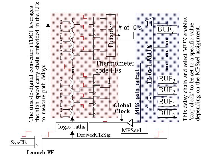
This is a diagram of the circuit that I would like to build initially. If I get this to work, then there are some other components I would add. This is a time-to-digital-converter (TDC) that uses the embedded, high speed carry chain to measure path delays along paths in the 'logic paths' block (not drawn to scale). The SysClk drives a register on the bottom left that 'launches' a rising edge into 'logic paths' block AND into the delay chain on the right. The 'logic paths' rising edge emerges and then propagates along the carry chain in the adder at high speed. The MPS_path_output drives the clock to the thermometer code registers (declared in Quartus as a Global Clock so the clock tree is used). Once the MPS_path_output goes high, the Thermometer code FFs stop sampling. The MPSsel control bits to the MUX allow different tap points to be selected along the delay chain to account for different delays along the paths in the 'logic paths' block. The idea is to set the MPSsel bits so that the edge propagating along the carry chain is still propagating when the MPS_path_output goes high. This way, you get a sequence of 0's followed by 1's in the Thermometer code FFs. Counting the number of 0's give a relative measure of the delay of the path in the 'logic paths' block that is being measured. In order for this to work, each of the adder cells and corresponding Thermometer code FF must be in the same LE, i.e., routing directly from the LUT to the FF input, and not through a randomly placed buffer as it is doing.
Quartus traces back to MPSsel bit[0] and thinks this signal is a clock. I'd like to tell it that it is NOT a clock and rather the DerivedClkSig is the real clock.
- Mark as New
- Bookmark
- Subscribe
- Mute
- Subscribe to RSS Feed
- Permalink
- Report Inappropriate Content
What does the code for the 12-to-1 mux look like? There must be a reason why Quartus thinks it's a clock.
As for the extra buffer delays, if turning off optimize hold timing doesn't work and you can determine (from timing analysis most likely; look at a timing report on one of those paths that have the buffer in it) why the buffers are getting added, you could try using set_max[min]_delay SDC constraints to force short routing on those paths and avoid the additional delay. It wouldn't be too bad to use since you can use wildcards to constrain all of them.
#iwork4intel
- Mark as New
- Bookmark
- Subscribe
- Mute
- Subscribe to RSS Feed
- Permalink
- Report Inappropriate Content
Did you take a look at the Post-Fit View? This view shows how its implemented exactly on the device post fitting stage. From the code you sent, I do not see those xtra LCELL block in the Post-Fit view. Plus I used the Enable Fast Input/Output register assignment in the Assignment editor for the therm_reg register.
- Mark as New
- Bookmark
- Subscribe
- Mute
- Subscribe to RSS Feed
- Permalink
- Report Inappropriate Content
I'm looking at the Technology Map Viewer (Post-Fitting) option under Fitter (Place & Route). I found no such option 'Enable Input/Output register assignment' in the Assignment editor (from the long list of items presented). Only 'Fast Ouput register' which tells Quartus (according to my reading) to put the register in an I/O cell. What version of Quartus are you using? I'm using 18.1 Standard edition.
- Mark as New
- Bookmark
- Subscribe
- Mute
- Subscribe to RSS Feed
- Permalink
- Report Inappropriate Content
I'm giving up on trying to do this on an Altera part. Two weeks of pain and frustration is all that I can tolerate. I tried every option that made sense. I even tightened the timing constraint to point of failure but still Quartus insisted on keeping the buffers. I don't know how Abe created his version without the buffers, except perhaps you are using something other than Quartus??? To me, this buffer insertion is a total waste of resources. 128 LE are being used to do this (actually many more exist in the design) and for what? Perhaps this is a bug in 18.1? Something is not right! The TDC critically depends on these buffers NOT being there, so this is a failed attempt at building a PUF on Altera FPGAs.
- Mark as New
- Bookmark
- Subscribe
- Mute
- Subscribe to RSS Feed
- Permalink
- Report Inappropriate Content
Have you tried the "Ignore LCELL buffers" constraint in the Assignment editor? This will tell the compiler to ignore LCELLs.
- Mark as New
- Bookmark
- Subscribe
- Mute
- Subscribe to RSS Feed
- Permalink
- Report Inappropriate Content
- Subscribe to RSS Feed
- Mark Topic as New
- Mark Topic as Read
- Float this Topic for Current User
- Bookmark
- Subscribe
- Printer Friendly Page


