- Mark as New
- Bookmark
- Subscribe
- Mute
- Subscribe to RSS Feed
- Permalink
- Report Inappropriate Content
Hello everybody
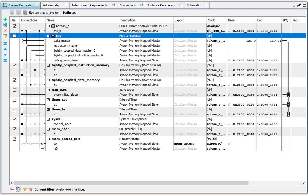
i have been now struggling for a week. I have a Qsys design, with nios2/f, ddr3 and onchip memory. I have implemented a tightly coupled instruction and data bus.
I can compile and download my firmware with no problem. When i download nios2 software i can see that it is downloaded and also it is running. All the messages are displayed in the nios2 command line.
What i want to do now is add a n external port so that i can write to ddr3 directly. I tried the avalon master template and it doesnt work. I wrote my own vhdl file that is very simple
library ieee;
use ieee.std_logic_1164.all;
use ieee.numeric_std.all;

entity mem_access is

  generic (
    BYTEENABLEWIDTH : integer := 4;     -- byte enable width
    ADDRESSWIDTH    : integer := 32;    -- width of the address bus
    DATAWIDTH       : integer := 32);   -- width of data bus

  port (
    csi_mem_clk          : in  std_logic;  -- clock of the memory controller
    csi_mem_reset_n      : in  std_logic;  -- reset of the memory controller
    avm_mem_waitrequest_n: in  std_logic;  -- wait request issued by memory
	avm_mem_beginbursttransfer : out std_logic;  -- read command to the memory
    avm_mem_address      : out std_logic_vector(ADDRESSWIDTH-1 downto 0);  -- address of the data in the memory
    avm_mem_readdatavalid: in  std_logic;  -- wait request issued by memory
	avm_mem_readdata     : in  std_logic_vector(DATAWIDTH-1 downto 0);  -- read data from memory
    avm_mem_writedata    : out std_logic_vector(DATAWIDTH-1 downto 0);  -- write data to the memory
    avm_mem_byteenable   : out std_logic_vector(BYTEENABLEWIDTH-1 downto 0);  -- byte to write to memory
    avm_mem_read         : out std_logic;  -- read command to the memory
    avm_mem_write        : out std_logic;  -- write command to the memory
    avm_mem_burtscount   : out std_logic_vector(DATAWIDTH/4-1 downto 0);  -- byte to write to memory

    cso_ctrl_clk         : in std_logic;  -- out clock from the NIOS fabric
    rso_ctrl_reset_n     : in std_logic;  -- out reset from the NIOS fabric
    avs_mem_writedata   : in  std_logic_vector(DATAWIDTH-1 downto 0);  -- data to be written from FPGA fabric
    avs_mem_readdata    : out std_logic_vector(DATAWIDTH-1 downto 0);  -- read data from memory
    avs_mem_burtscount   : in std_logic_vector(DATAWIDTH/4-1 downto 0);  -- byte to write to memory
    avs_mem_beginbursttransfer : in std_logic;  -- read command to the memory
    avs_mem_readdatavalid: out  std_logic;  -- wait request issued by memory
	avs_mem_address     : in  std_logic_vector(ADDRESSWIDTH-1 downto 0);  -- address of the data in the memory
    avs_mem_byteenable  : in  std_logic_vector(BYTEENABLEWIDTH-1 downto 0);  -- byte to write to memory
    avs_mem_write       : in  std_logic;  -- write command to the memory
    avs_mem_read        : in  std_logic;  -- read command to the memory
    avs_mem_waitrequest_n : out std_logic   -- wait request issued by memory
    );
end entity mem_access;

architecture top of mem_access is

begin  -- architecture top

  avs_mem_waitrequest_n <= avm_mem_waitrequest_n;
  avm_mem_beginbursttransfer <= avs_mem_beginbursttransfer;
  avm_mem_address      <= avs_mem_address;
  avs_mem_readdatavalid <= avm_mem_readdatavalid;
  avs_mem_readdata    <= avm_mem_readdata;
  avm_mem_writedata    <= avs_mem_writedata;
  avm_mem_byteenable   <= avs_mem_byteenable;
  avm_mem_read         <= avs_mem_read;
  avm_mem_write        <= avs_mem_write;
  avm_mem_burtscount <= avs_mem_burtscount;


end architecture top;
The slave port "avs_" is exported and master port "avm_" is connected directly to ddr3.
Can some one please tell me what i am doing wrong.
In Nios2 software i declare
volatile int* volatile pFlag = (int*)0x03000000;This is my address to which i want to write from vhdl. Then in the NIOS2 i check if the flag is 1 or 0.
The check show that 1pFlag is always 0.
I dont know why.
Did anyone try anything similar. How did you resolve this problem?
Thank you
Link Copied
- Mark as New
- Bookmark
- Subscribe
- Mute
- Subscribe to RSS Feed
- Permalink
- Report Inappropriate Content
It's not clear how you want to access the DDR3 from outside the system, but instead of the custom component you've created, use a pipeline bridge. You'll set it up basically the same as what you've created here (export the slave side; connect the master side to the slave memory interface).
- Mark as New
- Bookmark
- Subscribe
- Mute
- Subscribe to RSS Feed
- Permalink
- Report Inappropriate Content
Thank you very much for the answer
Pipeline bridge has master, slave and clk/rest port. It is not clear to me if clk/rst is used for both master and slave or only for slave.
Which of the two ports in pipeline bridge (master or slave) are clocked by the clk and rst port?
Thank you
- Mark as New
- Bookmark
- Subscribe
- Mute
- Subscribe to RSS Feed
- Permalink
- Report Inappropriate Content
Clock and reset are for the bridge itself, so both interfaces (master and slave). Just use the same clock and reset you're using for other components.
- Mark as New
- Bookmark
- Subscribe
- Mute
- Subscribe to RSS Feed
- Permalink
- Report Inappropriate Content
Hi
thank you very much for your suggestion. It work fine and it is much easier with pipeline bridge then what i had i mind. I also added a clock crossing bridge since my logic out side nios doesnt run on the same clock as NIOS.
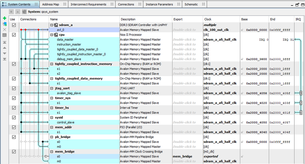
I have a system here with Cyclone V and 2G DDR3. There is some other periphery there also but i will leave it out for a moment.
Here is a picture of my system
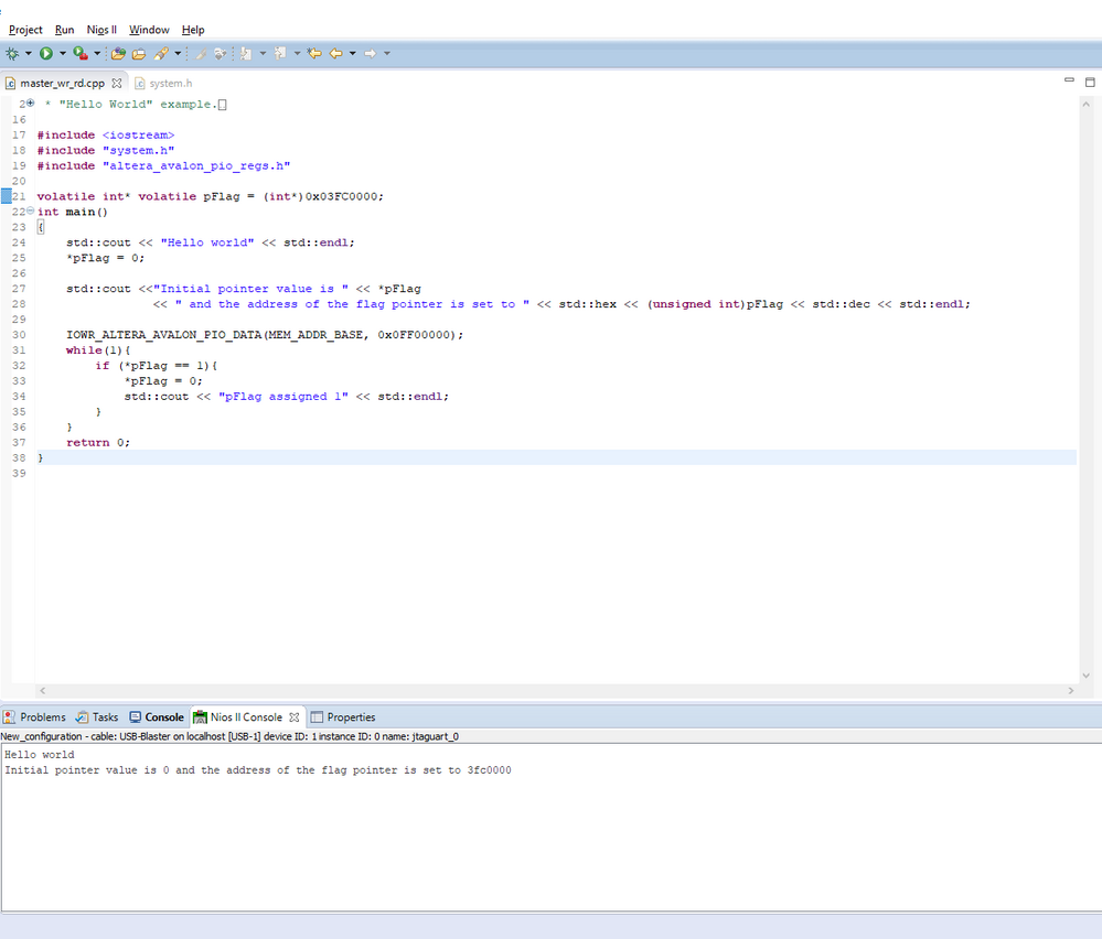
DDR3 is addressed from 0x0000_0000 to 0x0FFF_FFFF. This is the addressing of bytes, 0x0FFF_FFFF is 268KBytes which makes it 2Gbits. So that is fine. In NIOS software i declare a volatile pointer of int to address 0x0FF0_0000. Further more i initialize the value of this address to 0. When i run my nios software, in the command line i can see that value at the address to which pointer is pointing is correctly setup to 0, and also the address of the pointer is 0x0FF0_0000.
My external logic is setup such that every second a 1 is written to 0x0FF0_0000. So very second i expect NIOS software to write me "pFlag assigned 1". But that never happens. I tried looking at the signal tap to seewhat is going on
mem_bridge is the interface port to my logic, while qsys_system_sdram, is the qsys generated logic. From the picture you can see that when signal mem_bridge_write=1, mem_abridge_address=0x0FF0_0000, mem_bridge_byteenable=0xF, mem_bridge_writedata=1, mem_bridge_burstcount=1 and waitrequest is low. Accordig to the instructions those are to conditions for a valid write. About 20 clocks later you can see that simillar signal config is also on the sdram controller. The only difference that i see is in the address. IT looks like the address is shifted to bit down. I figure that is because sdram controller does addressing in 32-bit mode while bridges the do everything in 8 bit mode.
However i am still out cold. My while loop never gives me a message sayting that flag was set to 1.
I dont know what i am doing wrong, does someone have any ideas.
Thank you
- Subscribe to RSS Feed
- Mark Topic as New
- Mark Topic as Read
- Float this Topic for Current User
- Bookmark
- Subscribe
- Printer Friendly Page


