- Mark as New
- Bookmark
- Subscribe
- Mute
- Subscribe to RSS Feed
- Permalink
- Report Inappropriate Content
Hi all,
I have something very strange happening. I have programmed a Altera 7000 Series EPM7064 device. In it I created 4*6 bits register. Simulation is all good. Reset, writing and reading is all good.
Only in real life, checked with my Logic Analyser, I see the write but a microsecond later the value of the register does not appear on the output pins. Instead only zeroes appear.
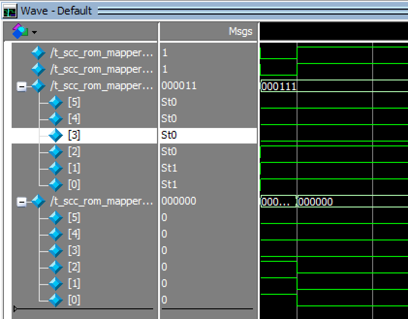
Here the output of the simulator:
At the bottom is the input data, all 3 lower bits high. In the middle the output of the register is written because WR and EN is low. And after writing it stays visible on the output pins [2][1][0].
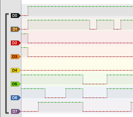
Here the output of the programmed device with the logic analyser:
The data D5/D6/D7 briefly appears at D2/D3/D4 and then goes back to zero and it stays that way.
Here the Verilog code:
module scc_rom_mapper (wr_n,sltsl_n,reset_n,a15_a13_a12,data,address_upper);
input [2:0] a15_a13_a12;
input [5:0] data;
input wr_n,sltsl_n,reset_n;
output reg [5:0] address_upper = 0;
// 4*6 bits storage
reg [5:0] mem0 = 6'b000000;
reg [5:0] mem1 = 6'b000001;
reg [5:0] mem2 = 6'b000010;
reg [5:0] mem3 = 6'b000011;
wire WE;
assign WE = !reset_n || (!sltsl_n && !wr_n);
// write memory
//////////////////
always @(posedge WE) begin
if (!reset_n) begin
mem0 <= 6'b000000;
mem1 <= 6'b000001;
mem2 <= 6'b000010;
mem3 <= 6'b000011;
end
if (!sltsl_n) begin
// store only when upper 4k is selected
case(a15_a13_a12)
3'b001: mem0 <= data;
3'b011: mem1 <= data;
3'b101: mem2 <= data;
3'b111: mem3 <= data;
default: ;
endcase
end
end
// read memory
////////////////////////
always @(*) begin
// always select correct bank when reading or writing
case(a15_a13_a12[2:1])
2'b00: address_upper <= mem0;
2'b01: address_upper <= mem1;
2'b10: address_upper <= mem2;
2'b11: address_upper <= mem3;
endcase
end
endmodule
Link Copied
- Mark as New
- Bookmark
- Subscribe
- Mute
- Subscribe to RSS Feed
- Permalink
- Report Inappropriate Content
It's not clear which signals are which in your simulation or your scope picture. Can you clarify?
And your coding for the "clock", WE, is strange. Do sltsl_n or wr_n toggle high/low for a write?
Also, you need an "else" on your check of sltsl_n in order to correctly code a register:
if (!reset_n) begin
.
.
.
else if (!sltsl_n)
Finally, it might be cleaner to code a 4x6 array instead of separate registers like this:
reg [5:0] mem [0:3];
#iwork4intel
- Mark as New
- Bookmark
- Subscribe
- Mute
- Subscribe to RSS Feed
- Permalink
- Report Inappropriate Content
In my design for an old retro computer project. I allow WRite when the SLot is SELected. I tried earlier an always (*) block with if/else statements but this wouldn't work. Hence the "clock" type of setup.
BTW. I did solve the issue at hand, being that the address_upper lines are cleared and not showing mem.
Somehow the reg[x] mem [x] initialisation was done at every evaluation. After putting this in an initial begin/end block this was solved.
So problem gone. ;-)
- Mark as New
- Bookmark
- Subscribe
- Mute
- Subscribe to RSS Feed
- Permalink
- Report Inappropriate Content
Hi Mario,
What I understand the control signal in your case is sltsl_n(sel) and wr_n(wr) should be toggling. The register is written when sltsl_n and wr_n is high on same clock edge. It return the current data when sltsl_n is high and wr_n is low. Using if else statement for this process as shown below is snippet sample.
always @ (posedge clk) begin
if (!rstn)
register <= 0;
else begin
if (sel & wr) // when both signal is high
register <= wdata; // non-blocking statement wdata assigned to register
else
register <= register;
end
end
- Subscribe to RSS Feed
- Mark Topic as New
- Mark Topic as Read
- Float this Topic for Current User
- Bookmark
- Subscribe
- Printer Friendly Page

