- Mark as New
- Bookmark
- Subscribe
- Mute
- Subscribe to RSS Feed
- Permalink
- Report Inappropriate Content
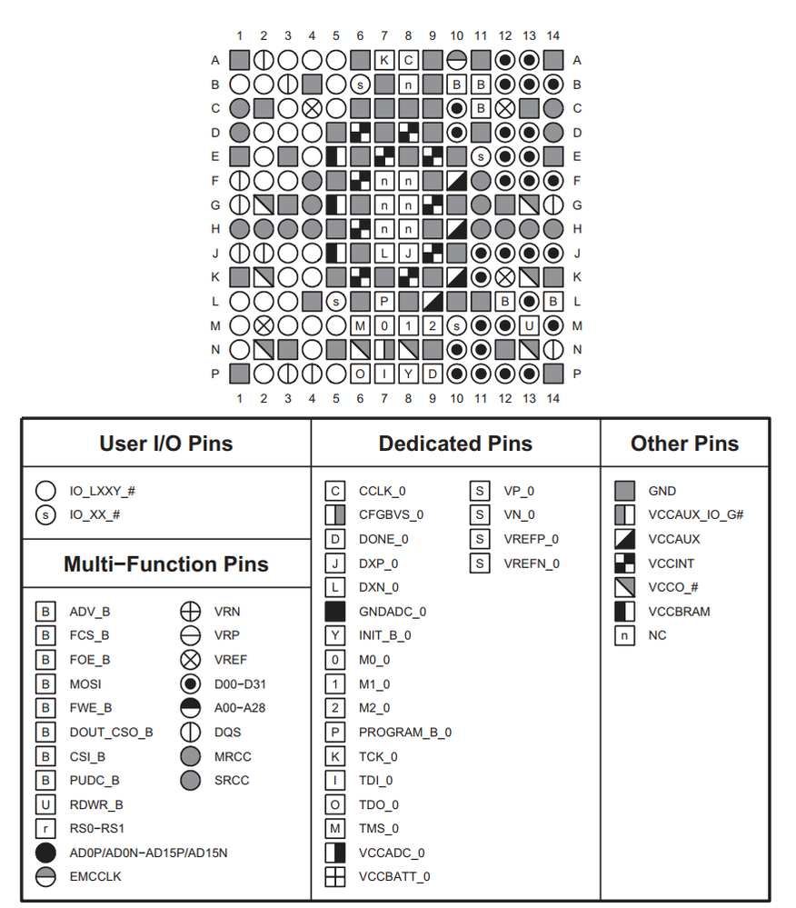
When doing FPGA pin placement it is useful to have an image with overview of available pins on the package, to use pins in a way that reduce PCB routing. An example for is shown below for a non-Intel FPGA.
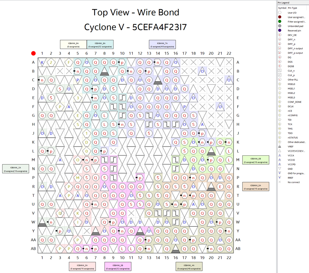
However, I have been unable to find a similar pin image overview of for example a Cyclone V FPGA device.
Is there any Intel FPGA documentation that gives an overview of the pins on the package on for example a Cyclone V FPGA device ?
Thanks in advance.
Image below shown pin location for a non-Intel FPGA.
Link Copied
- Mark as New
- Bookmark
- Subscribe
- Mute
- Subscribe to RSS Feed
- Permalink
- Report Inappropriate Content
The Pin Planner tool from the Assignments menu in Quartus shows this exact view for performing pin placement and creating other I/O-related assignments.
- Mark as New
- Bookmark
- Subscribe
- Mute
- Subscribe to RSS Feed
- Permalink
- Report Inappropriate Content
Thanks, that is definitely usable for specific projects.
Was able to get this nice picture, for reference:
- Mark as New
- Bookmark
- Subscribe
- Mute
- Subscribe to RSS Feed
- Permalink
- Report Inappropriate Content
I’m glad that your question has been addressed, I now transition this thread to community support. If you have a new question, feel free to open a new thread to get the support from Intel experts. Otherwise, the community users will continue to help you on this thread. Thank you.”
- Subscribe to RSS Feed
- Mark Topic as New
- Mark Topic as Read
- Float this Topic for Current User
- Bookmark
- Subscribe
- Printer Friendly Page

