- Mark as New
- Bookmark
- Subscribe
- Mute
- Subscribe to RSS Feed
- Permalink
- Report Inappropriate Content
Hi!
In our Arria10 device, transceiver phy is configured as below,
-Transceiver Configuration rules:Basic(Enhanced PCS)
-PMA configuration rules:basic
-Number of data channels:6
-Data rate:6144Mbps
-TX channel bonding mode:PMA and PCS bonding
-"Enable tx_pma_div_clkout port" is checked, division factor=33
We checked "Enable rx_seraillpbken port" and set to 1'b1 for serial loop back mode.
[result]
6 channels tx_control[1:0] are set to 2'b01.
But rx_control[1:0] of some channels are sometime different from 2'b01.
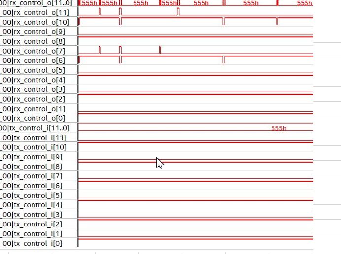
We attached the signal tap capture "WS000028.JPG"
WS0000028.JPG:
tx_control and rx_control signals are captured.
signal name description
tx_control[11:10]: tx_control[1:0] for channel 5
tx_control[ 9: 8]: tx_control[1:0] for channel 4
tx_control[ 7: 6]: tx_control[1:0] for channel 3
tx_control[ 5: 4]: tx_control[1:0] for channel 2
tx_control[ 3: 2]: tx_control[1:0] for channel 1
tx_control[ 1: 0]: tx_control[1:0] for channel 0
rx_control[11:10]: rx_control[1:0] for channel 5
rx_control[ 9: 8]: rx_control[1:0] for channel 4
rx_control[ 7: 6]: rx_control[1:0] for channel 3
rx_control[ 5: 4]: rx_control[1:0] for channel 2
rx_control[ 3: 2]: rx_control[1:0] for channel 1
rx_control[ 1: 0]: rx_control[1:0] for channel 0
Why are tx_control and rx_control not same ?
We suspect transceiver PHY reference clock jitter.
Cloud you tell reconfirm point ?
BR,
taira
Link Copied
- Mark as New
- Bookmark
- Subscribe
- Mute
- Subscribe to RSS Feed
- Permalink
- Report Inappropriate Content
Hi Taira,
From your signal_tap result, rx_control [5:0] looks fine while rx_control[11:6] result looks bad.
- Is this failure trend consistent meaning failure always occurs on rx_control[11:6] ?
- I presume the mapping is transceiver channel [2:0] is good while transceiver channel [5:3] is bad ?
Yes, transceiver clocking performance could be a concern here.
- Does resetting NativePHY IP helps to resolve the issue ?
- I presume you are using fPLL ? Is the fPLL sitted closer to channel [5:3] or [2:0] ? Does changing to other fPLL helps to resolve the issue here ?
- Also are you using dedicated refclk pin to clock the fPLL ? Else pls take note of below KDB known issue
- https://www.intel.com/content/www/us/en/programmable/support/support-resources/knowledge-base/tools/2017/fb470823.html
- You can try reduce the data rate from 6G to lower data rate to see if it helps
- You can also compared the CDR lock status signal (rx_is_lockedtodata) between good channel and bad channel to see id CDR loose lock is causing the issue here
- Finally pls measure the on board transceiver PLL refclk pin and CDR refclk pin clocking signal to ensure the clock source is clean and stable
Thanks.
Regards,
dlim
- Mark as New
- Bookmark
- Subscribe
- Mute
- Subscribe to RSS Feed
- Permalink
- Report Inappropriate Content
Hi, dlim
Thank you for your Information.
I want to confirm your check points, But My office is closed for COVID-19.
Maybe, until 6-May-2020.
So I will reply, when I can confirm .
Thanks.
BR,
Taira
- Mark as New
- Bookmark
- Subscribe
- Mute
- Subscribe to RSS Feed
- Permalink
- Report Inappropriate Content
Hi Taira,
No problem. I will keep the case open and waiting for your update in May.
FYI... Malaysia is impacted by COVID-19 as well. I have been working from home and fully understand your pain point from not able to work from office.
Thanks.
Regards,
dlim
- Mark as New
- Bookmark
- Subscribe
- Mute
- Subscribe to RSS Feed
- Permalink
- Report Inappropriate Content
Hi dlim,
Japan is impacted too.
I confirm that "I presume you are using fPLL ? Is the fPLL sitted closer to channel [5:3] or [2:0] ? Does changing to other fPLL helps to resolve the issue here ?"
My FPGA design has 4 instances of the module is included 6CH native PHY.
This issue is occured in one instance of them.
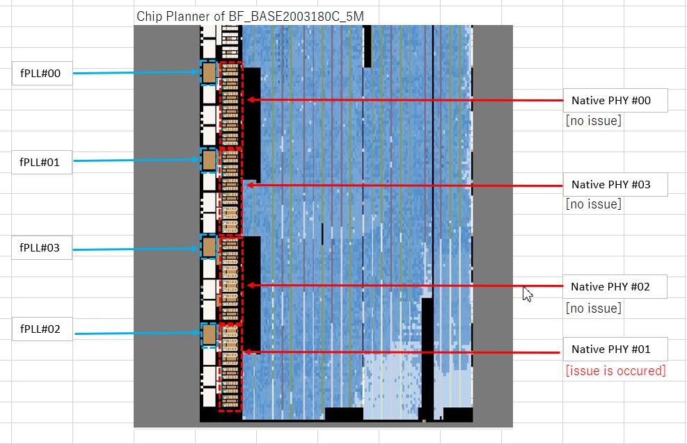
I attach Chip Planner view with comment(.
About Chip Planner view
the issue is occured in #01.
fPLL and Native PHY in the instance #01 are not located in the same bank.
I expect fPLL and Native PHY in the same instance are located in the same bank.
Is this fitting result a resonable ?
Should I modify FPGA configuration(qsf or sdc and so on) ?
Thanks.
BR,
Taira
- Mark as New
- Bookmark
- Subscribe
- Mute
- Subscribe to RSS Feed
- Permalink
- Report Inappropriate Content
Hi Taira,
Thanks for sharing the chip planner view. I have edit with comment and attached back for your reference.
- Sorry but it's unclear to me why are you saying fPLL#2 and NativePHY#01 doesn't belong to the same bank ? The chip planner shown that both are located on same bank, right ?
- Have you try to perform more debug on fPLL#2 as I suggested earlier ? Check the fPLL#2 on board clocking to ensure it's clean and stable, monitor fPLL#2 lock signal
- Also is there any fPLL on the same bank that you can try out by moving the PLL refclk pin to another bottom dedicated refclk pin on the same bank ?
- Lastly, how many failure boards that you see so far ? Does this failure happens on all your boards or just few boards ? This will helps us understand whether the issue is with hardware board/FPGA or Quartus design
Thanks.
Regards,
dlim
- Mark as New
- Bookmark
- Subscribe
- Mute
- Subscribe to RSS Feed
- Permalink
- Report Inappropriate Content
Hi Dlim,
Sorry for late reply. It was a national holidy from 29-April to 6-May.
1.Sorry but it's unclear to me why are you saying fPLL#2 and NativePHY#01 doesn't belong to the same bank ? The chip planner shown that both are located on same bank, right ?
Ans:fPLL#02 and NativePHY#01 are located on same bank.
In my RTL code, fPLL#i is used for Native PHY#i. So fPLL#02 is not used for Native PHY #01, but is used for Native PHY#02.
Is this answer enough to your quesstion ?
2.Have you try to perform more debug on fPLL#2 as I suggested earlier ? Check the fPLL#2 on board clocking to ensure it's clean and stable, monitor fPLL#2 lock signal
Ans:No, I haven't. It is extended to close office until 31-May. So I can not go my office.
3.Also is there any fPLL on the same bank that you can try out by moving the PLL refclk pin to another bottom dedicated refclk pin on the same bank ?
Ans:My hardware board has two dedicated refclk pin at "bank 1D". One is used, another one is not used. The one refclk pin is distributd to four fpLLs in 4 banks.
I will try, when I will be able to go to office.
4.Lastly, how many failure boards that you see so far ? Does this failure happens on all your boards or just few boards ? This will helps us understand whether the issue is with hardware
board/FPGA or Quartus design
Ans: I see two boards. The boards are prototype and was produced only two.
I think that fpLL#i and Native PHY#i should be located on the same bank.
But Qurartus Prime located to different bank.
I am worried that the definition in user SDC file or qsf file are not enough.
Is my understand about fpLL and Native PHY location correct or not?
Thanks.
BR,
taira
- Mark as New
- Bookmark
- Subscribe
- Mute
- Subscribe to RSS Feed
- Permalink
- Report Inappropriate Content
HI Taira,
Ok. Now I understand your issue better.
- By right we expect Quartus fitter to assign fPLL and transceiver channel on the same bank.
- But you are seeing fitter doesn't assign fPLL and transceiver channel on the same bank.
For hard debug, sure, I can wait for you to go back office to test it out after May 31.
For now, maybe you can help me understand your expected fPLL and transceiver channel placement first ?
- Based on chip planner view, I would expect
- fPLL#0 + NativePHY#0
- fPLL#1 + NativePHY#3
- fPLL#3 + NativePHY#2
- fPLL#2 + NativePHY#1
- But you mentioned you expect below combination ?
- fPLL#0 + NativePHY#0
- fPLL#1 + NativePHY#1
- fPLL#2 + NativePHY#2
- fPLL#3 + NativePHY#3
May I suggest you to edit your Arria 10 device pin out file to show me which fPLL refclk pin and transceiver channel that you set in Quartus qsf vs what's the actual pin placement that Quartus fitter set ? This will help me understand the overall pin placement issue better.
Also, did you configure the clocking network to x1 so that Quartus can try to fit both fPLL and transceiver channel into same bank ?
Thanks.
Regards,
dlim
- Mark as New
- Bookmark
- Subscribe
- Mute
- Subscribe to RSS Feed
- Permalink
- Report Inappropriate Content
Hi Dlim,
I think that you understand my expected placement about fPLL and Native PHY.
I attached excel file you suggested.
I seem that the pin placement in qsf is same as the pin placement in pin.rpt(actual).
Row P:User Pin assign from qsf
Row Q:Actual Pin assign from pin file
I don't configure the clocking network to x1, but "bonded x6".
I had additional questions, when I edited an excel file.
I configure pins as below.
-reference clock:I/O standard=LVDS
-transceiver PHY output:I/O standard=High Speed Differntial I/O
-transceiver PHY input:I/O standard=Current Mode Logic(CML)
I refer below URL
In section 5.1.1.2, transmitter buffer should be "High Speed Differential I/O".
In section 5.1.2.1, receiver can be selected High Speed Differential I/O or CML or Differential LVPECL or LVDS.
Which I/O standard should I select ?
I can not find the DC specification about High Speed Differential I/O,CML ,Differential LVPECL ,LVDS.
BR,
taira
- Mark as New
- Bookmark
- Subscribe
- Mute
- Subscribe to RSS Feed
- Permalink
- Report Inappropriate Content
Hi Dlim,
I want to update information.
I reduced the instance from #00,01,02,03 to #01.
As a result, the placement of fPLL was changed.
fPLL#01 was moved to below one bank.
I attached the chip planner view.
Does it mean that I can set the placement about fPLL by Quartus Prime ?
BR,
taira
- Mark as New
- Bookmark
- Subscribe
- Mute
- Subscribe to RSS Feed
- Permalink
- Report Inappropriate Content
HI Taira,
Sorry, I haven't got chance to review all your latest update yet.
We used to be able to fix fPLL location using QSF "location" command. Refer to below link
- https://www.intel.com/content/www/us/en/programmable/support/support-resources/knowledge-base/solutions/rd08092011_447.html
- However, take note this is for older FPGA, not Arria 10 FPGA
- Anyway, you can give it a try on your Arria 10 project. Just checked for the fPLL node path in fitter report.
Thanks.
Regards,
dlim
- Mark as New
- Bookmark
- Subscribe
- Mute
- Subscribe to RSS Feed
- Permalink
- Report Inappropriate Content
HI Taira,
Did you manage to fix the fPLL location ?
Any update to share with me ?
Thanks.
Regards,
dlim
- Mark as New
- Bookmark
- Subscribe
- Mute
- Subscribe to RSS Feed
- Permalink
- Report Inappropriate Content
Hi Dlim,
Sorry for late reply.
I could go to my office at 28 May.
But I work for higher priority tasks now.
So I can not start your suggestions.
Maybe, It is 2 weeks to complete my higer priority tasks.
I will reply, when I will be able to start your suggestions.
BR,
Taira
- Mark as New
- Bookmark
- Subscribe
- Mute
- Subscribe to RSS Feed
- Permalink
- Report Inappropriate Content
Hi Taira,
Alright, understood your situation to move to other higher priority task but I also want to let you know I can't let this case idle or open for too long without activity.
May I suggest for us to close this forum case first while you focus on your higher priority task ?
Once you are free in future then you can file new forum thread (quoting continuous support from this case 04589214) then I can resume to support you again.
Thanks.
Regards,
dlim
- Mark as New
- Bookmark
- Subscribe
- Mute
- Subscribe to RSS Feed
- Permalink
- Report Inappropriate Content
Hi Taira,
I hope you are fine with my suggestion to close this case first while you focus on your higher priority task.
I am now setting this case to closure first.
Feel free to file new forum thread to resume the debug discussion again in future.
Thanks for your understanding.
Regards,
dlim
- Subscribe to RSS Feed
- Mark Topic as New
- Mark Topic as Read
- Float this Topic for Current User
- Bookmark
- Subscribe
- Printer Friendly Page