- Mark as New
- Bookmark
- Subscribe
- Mute
- Subscribe to RSS Feed
- Permalink
- Report Inappropriate Content
I am going through the shit documentation and this is confusing me a lot. Someone please help me get through this mess.
Question 1: Where is the 50MHz clock (what pin)?
Question 2: Where is the switch to select the 125MHz clock?
Please see attached image to understand why I'm getting confused.
---------------------------------------------------------------
Image1 : clocking_cycloneIVgx_transceiverkit
---------------------------------------------------------------
clearly there are 3 clock inputs:
clock input 1: 100MHz from PCIE (no confusion ; I also have pin number)
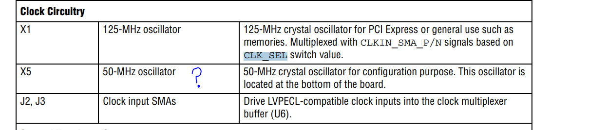
clock input 2: 50MHz clock show in image, but not in table 2-16 (where is this?)
clock input 3: 125MHz/SMA clock depending in CLK_SEL (okay...but where the hell is CLK_SEL?) Image 2 is related to this point.
---------------------------------------------------------------
Image 2 : dip_shit(switch)
---------------------------------------------------------------
There is supposed to be a physical switch on the board to help me select between SMA and on-board 125 MHz clock. Where is this switch???
Image 3 is related to this point
---------------------------------------------------------------
Image 3 : sma_clock_input
---------------------------------------------------------------
Where is this switch they are talking about? I removed the LCD panel. There ain't no switch?!?!?!
---------------------------------------------------------------
Image 3 : 50MHz_clock
---------------------------------------------------------------
Where is the 50-MHz clock??
Where is the CLK_SEL?
I'm even attaching the manual for your reference (and also as a sanity check that I'm not missing anything)
Really appreciate the time taken to sort this mess. How do they(intel/altera) expect someone to learn when there is lot of confusion in the documentation itself....is something that amazes me....anyways...any help appreciated
.PNG)
Link Copied
- Mark as New
- Bookmark
- Subscribe
- Mute
- Subscribe to RSS Feed
- Permalink
- Report Inappropriate Content
Hi,
Currently I am reviewing the forum for any open questions and found this thread. I apologize that no one seems to answer this question that you posted. Since it has been a while you posted this question, I'm wondering if you have found the answer? If not, please let me know, I will try to assign/find someone to assist you. Please do expect some delay in response as most of our agents are out of office due to the year-end holidays. Thank you.
Regards,
Nooraini
- Mark as New
- Bookmark
- Subscribe
- Mute
- Subscribe to RSS Feed
- Permalink
- Report Inappropriate Content
Hi,
Sorry for the delay. I might have overlooked this thread. As I understand it, you have some inquiries related to some clock sources in the CIV GX XCVR starter devkit. Please see my response to your inquiries as following:
Question 1: Where is the 50MHz clock (what pin)?
[Chee Pin] For your information, you may find the X5 oscillator in the page 5 of the starter kit schematic (c4gx_pcie_revb.pdf). the 50MHz goes into the PIN_A9 of the CIV GX device. Generally it is recommended to refer to the user guide for further details on the devkit component and pinout.
Question 2: Where is the switch to select the 125MHz clock?
[Chee Pin] For your information, the CLK_SEL is controlled by S8.1 dip switch. You may refer to Table 2–11. Board Settings DIP Switch Controls in the reference manual and page 5 of the schematic for further details.
Question 3: There is supposed to be a physical switch on the board to help me select between SMA and on-board 125 MHz clock. Where is this switch???
[Chee Pin] You may refer to the page 3 of the schematic for the dip switch location. You should look for dip switch S8 on the devkit.
Question 4: Where is this switch they are talking about? I removed the LCD panel. There ain't no switch?!?!?!
[Chee Pin] I believe you are referring to the physical location of the S8 dipswitch. For your information, as I checked with the devkit, it seems like the dipswitch is located at the back of the devkit. You may try to look at the back of the devkit for the S8 dipswitch.
Please let me know if there is any concern. Thank you.
Chee Pin
- Subscribe to RSS Feed
- Mark Topic as New
- Mark Topic as Read
- Float this Topic for Current User
- Bookmark
- Subscribe
- Printer Friendly Page