- Mark as New
- Bookmark
- Subscribe
- Mute
- Subscribe to RSS Feed
- Permalink
- Report Inappropriate Content
Hi everyone,
I just came across a very confusing thing about data arrival path in timing analyser. This path mismatched the actual routing path in the chip planner.
I placed a 20-bit adder between two registers which are clocked respectively at positive and negative edges. (I deliberately do this though it is not a good design practice.)
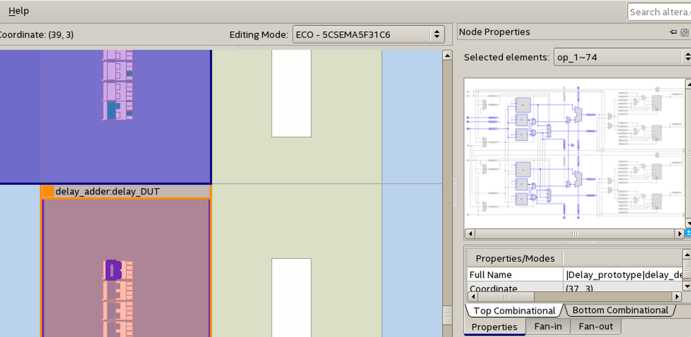
When I checked the placement and routing in the chip planner, I found all of fanouts and fanins are correct. The blue region in picture below shows that this 20-bit adder has been placed into 10 LABCELL blocks from its first bit adder to its last one.
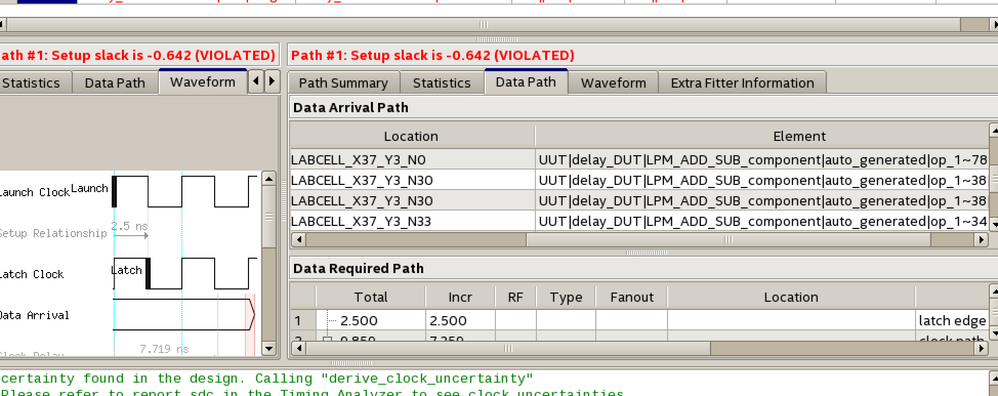
However, when I checked the timing analyser, a very confusing thing happened as shown in the screenshot below.
One could see clearly in the screenshot that the entry the first bit adder "LPM_ADD_SUB...|78" is NOT connected to "LPM_ADD_SUB....|op_1~74" which is the second bit adder, but connected to "LPM_ADD_SUB....|op_1~38". The delay path length of 20-bit adder is thus shrinking to only 11-bit according to the data arrival path in the timing analyser.
May I kindly ask has anyone come across similar situation before? Why the delay path in chip planner is not the same as shown in timing analyser.
Is it because routing of the 20-bit adder goes wrong? However, if it goes wrong, why fan-in and fan-out of each bit adder are correct?
Could anyone please kindly help me with this?
Thank you very much!
Mingqiang
Link Copied
- Mark as New
- Bookmark
- Subscribe
- Mute
- Subscribe to RSS Feed
- Permalink
- Report Inappropriate Content
Those are just names assigned by the tool, not physical resources. Check the Location column, not the Element column. There could also be optimizations happening depending on your implementation. And use the post-fit Technology Map Viewer for an easier to use view of how specific resources are connected together.
#iwork4intel
- Mark as New
- Bookmark
- Subscribe
- Mute
- Subscribe to RSS Feed
- Permalink
- Report Inappropriate Content
Hi sstrell,
Thank you for your help!
The first-bit adder is actually assigned myself using set_location_assignment (...)
These names actually matche the one in post-fit technology map, which I have attached for your references.
However, timing analyser shows that the data arrival path is not the same as the one in technology map viewer. If as you mentioned, they are just names, then the name in timing analyser indeed matches the one in technology map viewer and the one in .qsf file.
May I ask what is "location column"? Did you mean the resource property editor, or something else?
Thanks!
Mingqiang
- Mark as New
- Bookmark
- Subscribe
- Mute
- Subscribe to RSS Feed
- Permalink
- Report Inappropriate Content
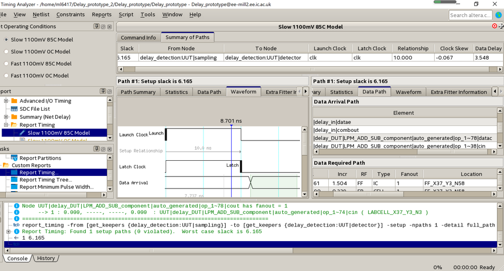
I mean the Location column in the Timing Analyzer, like what you show in the Data Required Path section in your first screenshot. Physical locations use a coordinate system: FF_X37_Y3_N58 for example.
#iwork4intel
- Mark as New
- Bookmark
- Subscribe
- Mute
- Subscribe to RSS Feed
- Permalink
- Report Inappropriate Content
Ah, I got your point. I have attached my newest timing analyser for your reference.
As you can see in the graph, the data goes from N0 to N30. However, in the chip planner's actual placement, it should go to N3 as shown in picture below. Op_1~74 is located in LABCELL...N3 and should be connected to the op 78 at N0.
Yet timing analyser shows different paths, meaning that connections from N3 to N27 goes wrong.
You can see my newst graph that i used logiclock region to constrain this adder but does not achieve what I want.
May I ask why the paths in chip planner and in timing analyser are different? How to solve this problem?
Thank you very much!
Mingqiang
- Mark as New
- Bookmark
- Subscribe
- Mute
- Subscribe to RSS Feed
- Permalink
- Report Inappropriate Content
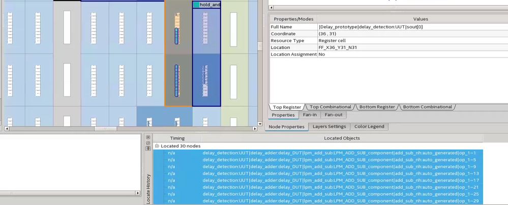
I'm not seeing what you're saying (and I don't see N27). The easiest way to correlate between the timing analyzer and the Chip Planner is to right-click the path in the timing analyzer and select Locate Path -> Locate in Chip Planner. This will show arrows in the Chip Planner that show connections. You'll also see the individual elements of the path in the Chip Planner in the Locate History section. Double-click any path in the Locate History to have it highlighted in the Chip Planner.
Also, since you are attempting manual placement of elements (usually not recommended), you should check compilation warnings to see if there are any issues with the placements you've made.
What is your ultimate goal here? Most folks don't go down to this level of detail for resource placement.
#iwork4intel
- Mark as New
- Bookmark
- Subscribe
- Mute
- Subscribe to RSS Feed
- Permalink
- Report Inappropriate Content
Hi there,
I will do the location as you suggested latter.
The aim of the design is testing delay of the adder. The method I used is an indircet one.
At gate level, to avoid any random placement, I have to place the components manually.
I ask the delay path mismatch here is because something strange occured during the test.
Theoretically, 20-bit adder delays more than 18-bit one if the input bit propagates to the last one. However, things go to the opposite that 20-bit adder delays less than 18-bit one, meaning that routing may go wrong.
I thereafter checked timing analyser, finding that there are some mismatches with the data path.
I therefore asked if anyone knows why this is the case. I highly suspect the compiler optimises some of the routing resources, but do not know how to preserve the routing.
May I ask if you have any ideas about manual routing of the adders or preserving the routing during retiming?
Thanks!
Mingqiang
- Mark as New
- Bookmark
- Subscribe
- Mute
- Subscribe to RSS Feed
- Permalink
- Report Inappropriate Content
Hi there,
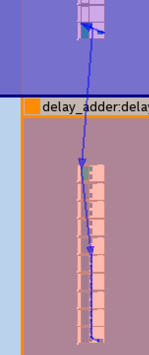
Thank you for the advice and after following this advice, I got the path below:
Indeed the routing does not go as I expected. You can see starting from the register in the blue area, it goes through a cell and goes to the first adder at the logic lock region "delay_adder".
Instead of traversing through the adder one by one, the arrow jumps to the 5th block where the 10th bit adder is located and then pass the next adder one by one until reaches the last register.
May I kindly ask how to constrain the route through all 20 bits of the adder?
Thank you!
Mingqiang
- Mark as New
- Bookmark
- Subscribe
- Mute
- Subscribe to RSS Feed
- Permalink
- Report Inappropriate Content
Hi Mingqiang,
There is no setting that you can control the routing of the design. You can set the location of the logic but not the routing path.
Thanks.
Best regards,
KhaiY
- Mark as New
- Bookmark
- Subscribe
- Mute
- Subscribe to RSS Feed
- Permalink
- Report Inappropriate Content
Hi KhaiY,
Thank you for your help!
I just found that only half of each LAB can be routed for each adder. Once the adder chain length is more than 10 bits, some bits will remain unrouted.
I do not know how to connect the whole 20-bit adder across 2 LABs without sharing arithmetic.
If you have ideas about it, I may ask you for suggestion!
Thank you very much!
Mingqiang
- Mark as New
- Bookmark
- Subscribe
- Mute
- Subscribe to RSS Feed
- Permalink
- Report Inappropriate Content
Hi Mingqiang,
Can you share the design.qar for investigation?
Thanks.
Best regards,
KhaiY
- Mark as New
- Bookmark
- Subscribe
- Mute
- Subscribe to RSS Feed
- Permalink
- Report Inappropriate Content
Hi KhaiY,
Thank you for your help!
I have already changed the design by adding flip-flops at the output of each adder.
Now Timing Analyser shows the path is correct.
However, real tests suggest that both Timing Analyser and chip planner does not tell the truth.
It looks like combinatorial adder can never be routed appropriately. I will probably abandon this design.
However, I can still sure the file for your reference. The problem is honestly strange!
Best Wishes,
Mingqiang
- Mark as New
- Bookmark
- Subscribe
- Mute
- Subscribe to RSS Feed
- Permalink
- Report Inappropriate Content
Hi Mingqiang,
I tried to locate all the sout in Chip Planner, all are located in 2 LABs.
Thanks.
Best regards,
KhaiY
- Mark as New
- Bookmark
- Subscribe
- Mute
- Subscribe to RSS Feed
- Permalink
- Report Inappropriate Content
Hi KhaiY,
Thank you for your help!
I did what you gave previously by putting them to two LABs, but the adders were still not fully connected. Let me explain this in a bit more detailed way.
The whole system is actually a testbench that tests the adders' combinatorial delay.
The one I gave you is a 30-bit adder which delayed certain amount.
I next cascaded a 20-bit one, with its first 10 bits constraining to the lower half of the first block and the next 10 bits constraining to the upper half of the second one.
However, this 20-bit adder delayed almost the same as the 30-bit one, meaning that some of the adders were not actually cascaded in the chain, although Timing Analyser said they were.
I also did another experiment that connected all adders' outputs to the HEX and LED displays on the DE1-SOC board. By setting one of the inputs of the adder 29'h1FFF_FFFF and another one to {29'h0, input}. If the "input" is 1, we will see only last LED is on and all the rest outputs goes to 0.
Unfortunately, the displayed pattern did not go as expected, meaning that the some of adders were not cascaded properly.
I will use oscilloscope to test them latter to find out whether the route goes wrong or something else goes wrong.
If you have the same DE1 board, maybe you can implement the my design on board to test if the delay is correct.
Thank you still for your help!
Best Wishes
Mingqiang
- Mark as New
- Bookmark
- Subscribe
- Mute
- Subscribe to RSS Feed
- Permalink
- Report Inappropriate Content
Hi Mingqiang,
Can you try to simulate the design and see if the signals give expected result?
Thanks.
Best regards,
KhaiY
- Mark as New
- Bookmark
- Subscribe
- Mute
- Subscribe to RSS Feed
- Permalink
- Report Inappropriate Content
Hi KhaiY,
Thank you for your method.
I guess the simulation you refer to is the gate-level simulation.
I had done RTL-level one before and the output sof the adder were correct.
I tried gate level simulation, but it did not give me any timing information about the cascaded length delay. I thus abandoned it.
I would double check the functionality simulation at this level latter. Nevertheless, since I will get an oscilloscope today, it is worth measuring the outputs to see the exact waveforms.
Thank you still for your concern! I will update what I found with you!
Best Wishes,
Mingqiang
- Mark as New
- Bookmark
- Subscribe
- Mute
- Subscribe to RSS Feed
- Permalink
- Report Inappropriate Content
Hi KhaiY,
Continuing from the gate-level simulation using Modelsim.
All ouptuts of the adders are correct as expected.
However, I still doubt whether gate-level simulation gives us correct functions in the real chip, though it is reliable to some extent.
I would use oscilloscope to do actual tests to find out what exactly has happened!
Thank you!
Mingqiang
- Mark as New
- Bookmark
- Subscribe
- Mute
- Subscribe to RSS Feed
- Permalink
- Report Inappropriate Content
Hi Mingqiang,
May I know if you have any updates?
Thanks.
Best regards,
KhaiY
- Mark as New
- Bookmark
- Subscribe
- Mute
- Subscribe to RSS Feed
- Permalink
- Report Inappropriate Content
Hi,
We do not receive any response from you to the previous question/reply/answer that I have provided. This thread will be transitioned to community support. If you have a new question, feel free to open a new thread to get the support from Intel experts. Otherwise, the community users will continue to help you on this thread. Thank you
Best regards,
KhaiY
- Mark as New
- Bookmark
- Subscribe
- Mute
- Subscribe to RSS Feed
- Permalink
- Report Inappropriate Content
Hi KhaiY,
I feel sorry to not response to you in time as I was so busy doing the experiment that I missed some of the messages previously.
Updating my situation: I used an oscilloscope to debug the adder, finding that neither Timing Analyser and chip planner tells the truth.
There was 30-bit adder connected when I implemented 32-bit adder.
Now I have found ways of solving the problem by removing all adders' inputs away. Instead, I connected these adders' inputs with a 10-bit switch.
Encoding the 10-bits to the number of input bits to adders, I have successfully cascaded a 96-bit adder and measured its delay time.
However, when I cascade more than 128-bit adders, testbench suggested that they may not be cascaded successfully. I am also currently finding out reasons and doing experiments.
It seems that the Quartus compiler connects adders in a very strange way between the inputs and the outputs.
What I do is probably very rare in FPGA and hence many bugs must be found via experiments.
Thank you very much for your concern! You can probably close this topic and label it solved.
Best Wishes,
Mingqiang
- Mark as New
- Bookmark
- Subscribe
- Mute
- Subscribe to RSS Feed
- Permalink
- Report Inappropriate Content
Hi Mingqiang,
Thanks for sharing the result of the experiment with oscilloscope. It is glad that you found the workaround. I now transition this thread to community support. If you have a new question, feel free to open a new thread to get the support from Intel experts. Otherwise, the community users will continue to help you on this thread. Thank you
Best regards,
KhaiY
- Subscribe to RSS Feed
- Mark Topic as New
- Mark Topic as Read
- Float this Topic for Current User
- Bookmark
- Subscribe
- Printer Friendly Page

