- Mark as New
- Bookmark
- Subscribe
- Mute
- Subscribe to RSS Feed
- Permalink
- Report Inappropriate Content
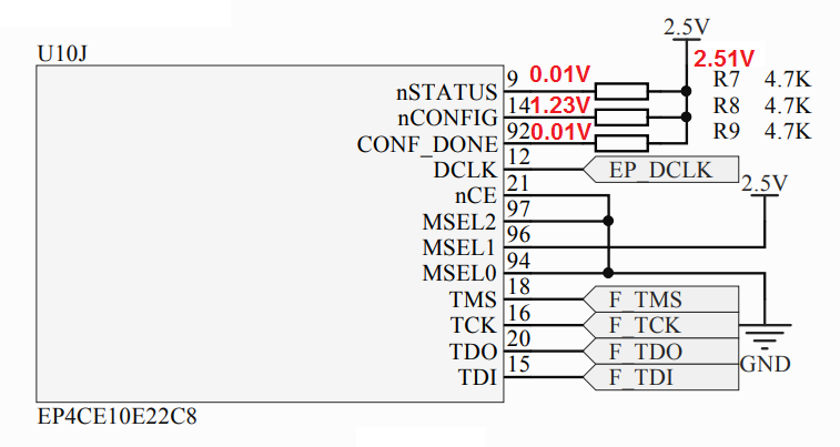
Hi I'm developing my own FPGA board using a Cyclone IV E EP4CE10E22C8N but when I use the USB blaster JTAG, it says it cannot scan the device chain. I have measured the configuration pin voltages (nSTATUS, nCONFIG, and CONFIG_DONE) and have found them to be 0V, 1.2V and 0V respectively. The hardware one each pin is a single series pull up resistor of 4k7 ohms to a 2.5V supply for each pin. Below is an excerpt from my schematic with measured voltages in red.
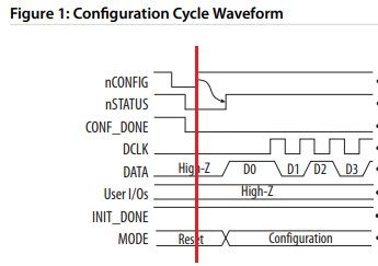
From "Figure 1: Configuration Cycle Waveform" on this Intel document (https://www.intel.com/content/dam/altera-www/global/en_US/pdfs/literature/hb/cfg/cfg_cf51001.pdf) I suspect I am stuck somewhere in the reset or early configuration section. Why this is I do not know.
I am puzzled why I see 1.2V on the nCONFIG pin, surely this ought to be either 0V or 2.5V?
One thing I feel might play a part is that these pins are pulled up to 2.5V, not the 3.3V I am using on my VCCIOx pins. This Intel document (https://www.intel.com/content/dam/altera-www/global/en_US/others/download/board-layout-test/schematic-review-ws/worksheets/Cyclone_IV_Schematic_Review_Worksheet.doc) on pgae 19 states that nCONFIG should be connected to VCCA (I believe 2.5V in this case) if a PS configuration scheme with a download cable is being used. However I am unsure what a PS configuration scheme and download cable specifically are.
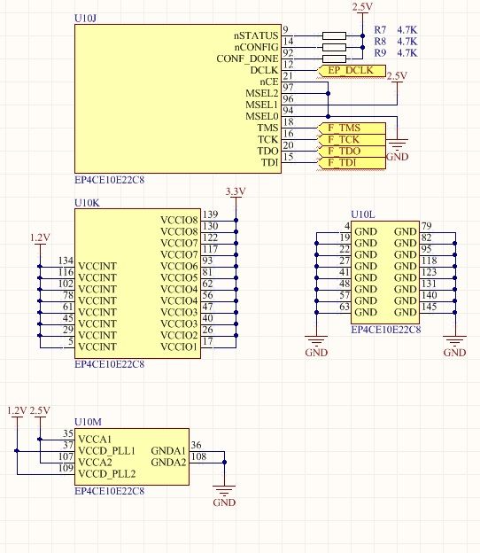
The same section states that nCONFIG should otherwise be connected to VCCIO (in my case 3.3V NOT 2.5V). Is this where I am going wrong? Before I alter my PCB I would like to check that this modification will not damage my FPGA or USB Blaster. Here is a larger section of my FPGA power and configuration portion.
Thanks in advance for your help.
Link Copied
- Mark as New
- Bookmark
- Subscribe
- Mute
- Subscribe to RSS Feed
- Permalink
- Report Inappropriate Content
Hi Ted,
As per your input, FPGA is in the reset state because POR requirement as not met.
After device power up, the device does not release nSTATUS until VCCINT, VCCA, and VCCIO (for I/O banks in which the configuration and JTAG pins reside) are above the POR trip point of the device. VCCINT and VCCA are monitored for brown-out conditions after device power up. Check the Device handbook/Datasheet for POR.
- Check if power(VCCINT, VCCA & VCCIO ) signals are properly power to its respective voltage within a specific time and share its status.
- Can't scan JTAG chain" error when trying to configure or Auto-Detect your Cyclone IV E.
- Are you using a development kit or custom board?
- check JTAG pins, Are they connected as per guidelines.
- Also, check the connection between Blaster & JTAG header.
Regards
Anand
- Mark as New
- Bookmark
- Subscribe
- Mute
- Subscribe to RSS Feed
- Permalink
- Report Inappropriate Content
Hi Anand,
Many thanks for your detailed response, I really appreciate the effort. In answer to each of your points:
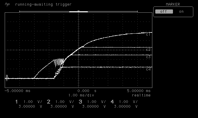
1) I measured the 4 voltages of interest (5V main supply, 3.3V for IO, 2.5V and 1.2V) during switch on. The waveforms are as follows:
Where c1 = 5V, c2 = 3.3V, c3 = 2.5V and c4 = 1.2V. The verticle scale is constant at 1V/div and the horizontal scale is also constant at 1ms/div. From the point the 5V supply turns on it takes only 1.2ms for the three FPGA supplies to start. From this point in time, the three supplies reach their rated voltages in just less than 2ms. From the Cyclone IV Device Datasheet (https://www.intel.com/content/dam/www/programmable/us/en/pdfs/literature/hb/cyclone-iv/cyiv-53001.pdf) page 1-5 states that:
"(5) The POR time for Standard POR ranges between 50 and 200 ms. Each individual power supply must reach the recommended operating range within 50 ms.
(6) The POR time for Fast POR ranges between 3 and 9 ms. Each individual power supply must reach the recommended operating range within 3 ms. "
I don't know if I'm configured for standard or fast POR, but evidently the <2ms POR meets both criteria.
2) The can't scan JTAG chain message appears when I attempt to use the "Auto Detect" button in the Programmer in Quartus Prime Lite Edition. I am not doing any other configuration steps before this - should I be?
3) This is a custom board.
4) I've checked the JTAG pins and am fairly sure they are correct. I've also checked to ensure there are no open connections or shorts here.
5) I believe the connection between Blaster and JTAG header is ok.
I am quite puzzled by the 1.2V state on the nCONFIG pin. As it is pulled up to 2.5V, surely it should be at either 0V or 2.5V in a normal logic state? Or is there additional behaviour? I have included my schematic as a pdf for your consideration. The main FPGA is presented on page 3. The JTAG header is on page 6, labelled as CON 11. My possible concern is that my supply voltages are not correct (including on JTAG) . What do you make of them? Below is a drawing of my JTAG connector (CON 11) as if you are looking into it. The notch is indicated for the Blaster connection.
Thanks again in advance.
- Mark as New
- Bookmark
- Subscribe
- Mute
- Subscribe to RSS Feed
- Permalink
- Report Inappropriate Content
Hi Ted,
As per the information provided, the POR requirement looks fine. Now we should focus on JTAG, regulator & passive component on board.
- Try to have 1K ohm resistors for JTAG header circuitry, I know Resistor value can vary from 1 k to 10 k, depending on the hardware it may change, try changing the values.
- What is the supply current of the 5V main supply ?? Because nConfig voltage as dropped, Voltage may drop if it can't drive enough current and ensuring power remains the same.
- Can you replace the 4K7ohm resistor on nConfig can check??
- Also, check power signals from the source till the destination pins(including regulator & passive component).
Regards
Anand
- Mark as New
- Bookmark
- Subscribe
- Mute
- Subscribe to RSS Feed
- Permalink
- Report Inappropriate Content
Hi Anand,
I have changed the resistors on the jtag header (R43, 44, 45) to 1k. I tested the device again, but not able to scan device chain.
I am fairly confident the 5V supply is ok, it is an Agilent E3631A which I have set with current protection at 500mA. The powersupply says about 50-60mA are being source from the 5V supply.
I replaced the 4k7 resistor on nConfig with a 10k resistor and the voltage read 0.8V. I then replaced it again with a 1k resistor and it now reads 2V. Still no luck.
I have checked continuity between voltage supplies and the FPGA pins - they are all fine.
Regards
- Mark as New
- Bookmark
- Subscribe
- Mute
- Subscribe to RSS Feed
- Permalink
- Report Inappropriate Content
Hi,
Is your vccio 3.3?? if yes
Pins must be connected directly or through a 10-KΩ resistor to VCCIO.
Regards
Anand
- Mark as New
- Bookmark
- Subscribe
- Mute
- Subscribe to RSS Feed
- Permalink
- Report Inappropriate Content
Hi Tbake8,
There are a few things that I think could be of issue. There has been a good back and forth between you and Anand, so forgive me for lack of continuity.
First, lets address your confusion about passive serial configuration. The FPGA can configure itself/be configured in a variety of ways. See chapter 8 of the Cyclone IV handbook to read about the differences between active configuration vs. passive configuration vs. JTAG configuration.
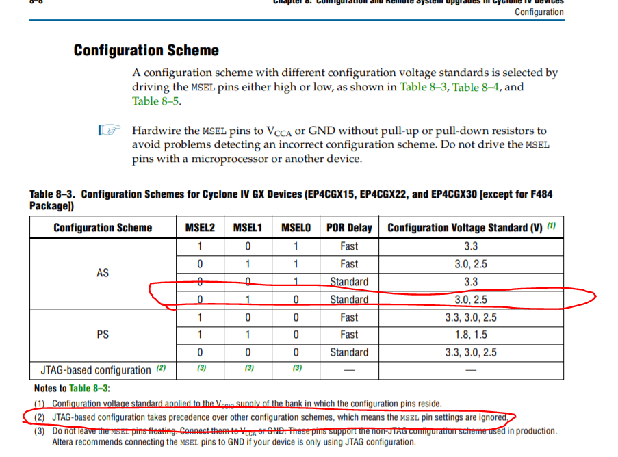
To not overcomplicate things, the way your FPGA is expecting to be configured is based on the MSEL pins. Based on your schematic your MSEL[2:0] pins are 010. This correlates to an active serial configuration method for your Cyclone IV device. See the below image, but your FPGA is expecting an active serial configuration scheme in the standard POR delay mode.
As to why you are seeing the strange voltage values on nCONFIG, I unfortunately cannot say right now.
But if you refer to the bottom of that image I posted, I circled another statement. What that statement is saying is: JTAG configuration should always work with this device, regardless of what your MSEL pins are. So that begs the question: “well why does JTAG config not work for me? When I try and “target” my device over the Quartus programmer, I can’t see the device.”
This is a good question, but I also am not sure at the current moment (☹). It looks like the pinout of your JTAG header (which is where the USB blaster plugs into) is correctly pinned out, but that is worth double checking. I think tackling and figuring out why you cant see your device over JTAG should be first priority. Then figuring out what is wrong with the nCONFIG, nSTATUS, and other related pins.
Also, be sure that Quartus Lite was correctly installed on your machine and that your drivers are up to date/correct.
Hope this was somewhat helpful.
- Mark as New
- Bookmark
- Subscribe
- Mute
- Subscribe to RSS Feed
- Permalink
- Report Inappropriate Content
Hi Ted,
Have you solved the problem?
The nCONFIG should be connected to VCCIO as mentioned in pin connection guidelines.
Regards
Anand
- Mark as New
- Bookmark
- Subscribe
- Mute
- Subscribe to RSS Feed
- Permalink
- Report Inappropriate Content
Hi Anand and Awein,
Apologies for disappearing for a few days... I was really banging my head against the wall. However, I found the solution. In a fit of despair I threw lots of extra solder and flux on the device, and it was recognised. I assume that at least one power pin was incorrectly soldered, but when applying pressure on the pin with my multimeter probe I was making the connection. Unfortunately, I cannot say which pin precisely was unsoldered, but there we have the culprit.
Thanks for both of your help and guidance. Hopefully if others have these strange issues with undefined vp;tages on pins, then they should double, triple check their soldering. :)
- Mark as New
- Bookmark
- Subscribe
- Mute
- Subscribe to RSS Feed
- Permalink
- Report Inappropriate Content
Thanks, ted.
the solution will help the community.
- Subscribe to RSS Feed
- Mark Topic as New
- Mark Topic as Read
- Float this Topic for Current User
- Bookmark
- Subscribe
- Printer Friendly Page
