- Mark as New
- Bookmark
- Subscribe
- Mute
- Subscribe to RSS Feed
- Permalink
- Report Inappropriate Content
I have a source-synchronous input to my Cyclone 10 GX (10CX085) FPGA, coming from an external chip whose datasheet gives the following information:
fmax = 300 MHz (single data rate)
tsetup = 0.4 ns
thold = 0.5 ns
Using an oscilloscope, I can see that the data is "center-aligned" (such that the data values are stable near the rising edge of the clock). Therefore, my interpretation of the datasheet is that the data is guaranteed to be stable for 0.9 ns per clock cycle (from 0.4 ns before the rising edge of the clock, until 0.5 ns after).
I have stripped my whole design down to two flip-flops (see attached quartus_project.zip) and I still struggle to meet timing, even if I heavily relax the timing constraints.
By closely following Intel's AN433 and free training course, I understand that for best timing performance I should instantiate a PLL (specifically, an IOPLL configured in "source synchronous" mode - green block above) and my timing constraints should be defined like this:
# Define input clock parameters
set period 3.333
set tsu 0.4
set th 0.5

# Define input delays
set half_period [expr $period/2]
set in_max_dly [expr $half_period - $tsu]
set in_min_dly [expr $th - $half_period]

# Create virtual launch clock
create_clock -name virtual_clock -period $period

# Create physical base clock (phase shifted by 180 degrees) on FPGA pin
create_clock -name Clk -period $period -waveform "$half_period $period" [get_ports Clk]

# Create generated clocks on the PLL outputs
derive_pll_clocks

# Set input delay constraints
set_input_delay -clock [get_clocks virtual_clock] -max $in_max_dly [get_ports InData*]
set_input_delay -clock [get_clocks virtual_clock] -min $in_min_dly [get_ports InData*]
This failed timing catastrophically, so I tried relaxing to a 10 MHz clock with an extremely generous thold = 25 ns:
# Define input clock parameters
set period 100
set tsu 0.4
set th 25
It surprised me that this also failed timing. Since the data is stable for >25 ns and I have told the tools when that stable time will be (relative to the phase of the 10 MHz clock), I thought maybe Quartus would be able to adjust delays (and/or PLL phase) to ensure the data is sampled near the middle of the "stable" time.
However, if I manually adjust the phase of the PLL (to basically anything sufficiently larger than zero) then timing is of course met comfortably on the 10 MHz clock:
This leaves me very confused about the following:
- Are my requirements (300 MHz, 0.5 ns, 0.4 ns) feasible with this device?
- If so, then how? (Timing contraints, PLL configuration, etc).
- If not, then what performance is possible? (I can't see this information anywhere in the 10CX085 documentation).
Many thanks in advance for any help.
- Mark as New
- Bookmark
- Subscribe
- Mute
- Subscribe to RSS Feed
- Permalink
- Report Inappropriate Content
The timing requirements can be met using PHY Lite. Unfortunately, the PHY Lite documentation is atrocious. This led to a protracted nightmare of failed Intel "support" here and then here.
Eventually, my company was somehow able to contact an engineer at Intel, who solved the problem immediately.
In summary:
- The refclk and strb pins (two FPGA pins) must both be driven by the same external clock.
- There is a bug in all versions of Quartus up to and including 21.4, which prevents the IO delay chains from being configured correctly. Therefore, the design will typically fail timing, even if everything has been configured correctly. As a workaround (until the bug is fixed in Quartus 22.1), the IO delay chains can be configured manually (see details below).
Here is the content of the (excellent) E-mail:
Quartus should automatically change the IO delay chain settings such that each IO is optimized for both setup and hold however there appears to be a problem with the automatic delay chain calculation algorithm in 21.3 which is why you are seeing lots of hold violations while your setup looks good.

I have checked in 21.4 and can confirm that the same issue exists in that version too.
I can however confirm that this issue has been resolved in the latest internal release of 22.1 which is due for release very soon.

As a temporary solution (prior to the release of 22.1) you can manually set the IO delay chain values using the assignment below.

set_instance_assignment -name IO_12_LANE_INPUT_DATA_DELAY_CHAIN 60 -to InData

You can apply this to all InData pins (as in the assignment above) however to get the optimum solution you will need to apply different values on a per-pin basis which is also supported.
I am looking at what specific settings are required to close timing and will update you in due course.

You can see the delay chain values used in the "Delay Chain Summary" section of the Route Stage report.

I tested the assignment above in 21.3 and the interface closed timing.

With regard to the refclk versus the strobe, ideally these should both originate from the same clock source such that they are PPM aligned. This will prevent the internal FIFO within the PHYLITE IP from overflowing/underflowing.
The simplest solution is to connect the same clock on your board to both the strobe and refclk pins of the device.
We applied these changes in our project and it met timing. Correct behavior has been confirmed in simulation.
Link Copied
- Mark as New
- Bookmark
- Subscribe
- Mute
- Subscribe to RSS Feed
- Permalink
- Report Inappropriate Content
When you say that it failed timing catastrophically, what exactly is failing? Can you show waveforms and numbers from the timing analyzer?
Your constraints look good. Does the -waveform with the Tcl variables in quotes work correctly? Normally those would be [] around the actual values.
- Mark as New
- Bookmark
- Subscribe
- Mute
- Subscribe to RSS Feed
- Permalink
- Report Inappropriate Content
@sstrell Thank you for your reply.
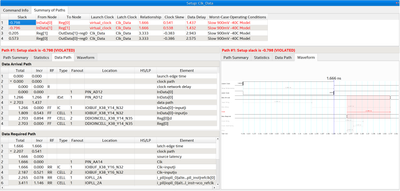
Both setup and hold timing fail on the first flip-flop. Here is the setup timing analysis:
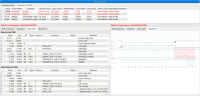
And here is the hold timing analysis:
As you can see in the Waveform panes, the -waveform SDC command is being picked up correctly (and there are no warnings about this). In the Intel examples that I used as a reference, they use curly braces to form a string literal {1.23 4.56}. I just used double quotes so I could evaluate variables "$var1 $var2" without having to delimit the $ with a \.
- Mark as New
- Bookmark
- Subscribe
- Mute
- Subscribe to RSS Feed
- Permalink
- Report Inappropriate Content
Everything you've done here looks correct, so I guess the device just can't meet those timing requirements. As you found, you could phase shift the clock with the PLL to latch the data later, but you'll probably need multicycle to line things up correctly.
- Mark as New
- Bookmark
- Subscribe
- Mute
- Subscribe to RSS Feed
- Permalink
- Report Inappropriate Content
The timing requirements can be met using PHY Lite. Unfortunately, the PHY Lite documentation is atrocious. This led to a protracted nightmare of failed Intel "support" here and then here.
Eventually, my company was somehow able to contact an engineer at Intel, who solved the problem immediately.
In summary:
- The refclk and strb pins (two FPGA pins) must both be driven by the same external clock.
- There is a bug in all versions of Quartus up to and including 21.4, which prevents the IO delay chains from being configured correctly. Therefore, the design will typically fail timing, even if everything has been configured correctly. As a workaround (until the bug is fixed in Quartus 22.1), the IO delay chains can be configured manually (see details below).
Here is the content of the (excellent) E-mail:
Quartus should automatically change the IO delay chain settings such that each IO is optimized for both setup and hold however there appears to be a problem with the automatic delay chain calculation algorithm in 21.3 which is why you are seeing lots of hold violations while your setup looks good.

I have checked in 21.4 and can confirm that the same issue exists in that version too.
I can however confirm that this issue has been resolved in the latest internal release of 22.1 which is due for release very soon.

As a temporary solution (prior to the release of 22.1) you can manually set the IO delay chain values using the assignment below.

set_instance_assignment -name IO_12_LANE_INPUT_DATA_DELAY_CHAIN 60 -to InData

You can apply this to all InData pins (as in the assignment above) however to get the optimum solution you will need to apply different values on a per-pin basis which is also supported.
I am looking at what specific settings are required to close timing and will update you in due course.

You can see the delay chain values used in the "Delay Chain Summary" section of the Route Stage report.

I tested the assignment above in 21.3 and the interface closed timing.

With regard to the refclk versus the strobe, ideally these should both originate from the same clock source such that they are PPM aligned. This will prevent the internal FIFO within the PHYLITE IP from overflowing/underflowing.
The simplest solution is to connect the same clock on your board to both the strobe and refclk pins of the device.
We applied these changes in our project and it met timing. Correct behavior has been confirmed in simulation.
- Subscribe to RSS Feed
- Mark Topic as New
- Mark Topic as Read
- Float this Topic for Current User
- Bookmark
- Subscribe
- Printer Friendly Page


