- Mark as New
- Bookmark
- Subscribe
- Mute
- Subscribe to RSS Feed
- Permalink
- Report Inappropriate Content
I need to design a source synchronous interface for high speed ADCs. I have not yet come across any Intel/Altera specific documentation on how to do this. If anything for this exists for Max 10 and Cyclone 10 LP then please let me know.
Link Copied
- Mark as New
- Bookmark
- Subscribe
- Mute
- Subscribe to RSS Feed
- Permalink
- Report Inappropriate Content
This page contains some information about Xilinx. However, there is nothing mentioned about Altera/Intel except a placeholder. Maybe Intel can help fill that in?
Source synchronous interface design with FPGAs [Analog Devices Wiki]
- Mark as New
- Bookmark
- Subscribe
- Mute
- Subscribe to RSS Feed
- Permalink
- Report Inappropriate Content
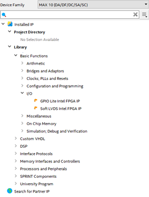
The Max 10 IP catalogue does not contain many I/O functions as can be seen here:
For example, ALTDDIO_IN, ALTDDIO_OUT and ALTIOBUF are all missing. I take this to mean that Max 10 does not have capability to be interfaced with a 120 MHz ADC via DDR LVDS mode. Is this correct?
- Mark as New
- Bookmark
- Subscribe
- Mute
- Subscribe to RSS Feed
- Permalink
- Report Inappropriate Content
HI,
There is Intel MAX 10 High-Speed LVDS I/O User Guide: https://www.intel.com/content/www/us/en/programmable/documentation/sam1394433606063.html#sam1394435208308 available to handle the high-speed ADC interface.
Regards.
- Mark as New
- Bookmark
- Subscribe
- Mute
- Subscribe to RSS Feed
- Permalink
- Report Inappropriate Content
I am a bit confused by your response. The SERDES is used to basically do a serial to parallel conversion on parallel data streams. In the case in the original post, the scenario is a parallel 12-bit source synchronous transfer. Xilinx has documentation on how to deal with this issue and use low level primitives blocks like IOBUF, IDELAY e.t.c. Therefore, it was natural for me to see how such buffers can be instantiated in Altera/Intel FPGA code. I then found that the ALTDDIO_IN, ALTDDIO_OUT and ALTIOBUF exist in Cyclone V but not MAX 10. This gave me the impression that source synchronous input of ADC will not work with the MAX 10.
The document your mentioned says that Max 10 implements SERDES in LEs. OK, but how does that related to the original problem I have mentioned about?
- Mark as New
- Bookmark
- Subscribe
- Mute
- Subscribe to RSS Feed
- Permalink
- Report Inappropriate Content
Hi,
The IP instantiates the DDIO by default.
It uses the clock coming in from ADC (rx_inclock), pass to the PLL to generate faster clock and use it to sample the DDR data at the rate defined by the PLL settings in IP wizard.
For a source synchronous ADC, Data rate will match the Inclock frequency in the PLL settings.
To define the data pins as LVDS, just assign the IO standard as LVDS in Pin planner, and it takes care of the LVDS buffers as well.
Regards.
- Mark as New
- Bookmark
- Subscribe
- Mute
- Subscribe to RSS Feed
- Permalink
- Report Inappropriate Content
This is well and good. But my question is, why are ALTDDIO_IN, ALTDDIO_OUT and ALTIOBUF not present in the IP catalogue of Max 10?
- Mark as New
- Bookmark
- Subscribe
- Mute
- Subscribe to RSS Feed
- Permalink
- Report Inappropriate Content
You can use the GPIO Lite Intel FPGA IP for DDIO. Please refer the documentation below:
Regards.
- Subscribe to RSS Feed
- Mark Topic as New
- Mark Topic as Read
- Float this Topic for Current User
- Bookmark
- Subscribe
- Printer Friendly Page
