- Mark as New
- Bookmark
- Subscribe
- Mute
- Subscribe to RSS Feed
- Permalink
- Report Inappropriate Content
I have a warning message that I don't why it appear. I use ALLPLL to generate other clocks. The output of PLL is from pll_c0 to pll_c5. Following's case are the case that I had tried at pll_c4.
Case(1):
assign pll_c4_sw = sel? pll_c4 : clk_pin;
Case(2):
assign pll_c4_sw = pll_c4;
Under case(1), I get the warning as following, and TimeQuest can't also find the pll_c4 to analysis. Can any tell me what happen there? Thank you.
Warning:
PLL "pll|altpll_component|auto_generated|pll1" has parameters clk4_multiply_by and clk4_divide_by specified but port CLK[4] is not connected.
TimeQuest TCL command:
create_generated_clock -name pll_c4 -source [get_pins pll|altpll_component|auto_generated|pll1|inclk[0]] -multiply_by 1 -divide_by 4 [get_pins pll|altpll_component|auto_generated|pll1|clk[4]]
Link Copied
- Mark as New
- Bookmark
- Subscribe
- Mute
- Subscribe to RSS Feed
- Permalink
- Report Inappropriate Content
It looks like you didn't enable CLK[4] in the PLL's parameter editor.
But also for your "case 1", you should use a clock control block IP to do clock network switching instead of this.
- Mark as New
- Bookmark
- Subscribe
- Mute
- Subscribe to RSS Feed
- Permalink
- Report Inappropriate Content
Hi sstrell, thank you very much.
I'm sure that I had enabled CLK[4] because TimeQuest can analysis the timing of CLK[4] in case(2), and the Verilog model file also define that it's used, like following picture.
verilog file of PLL:
Could you please tell me what clock control block IP can be used for clock network switching in case(1)?
- Mark as New
- Bookmark
- Subscribe
- Mute
- Subscribe to RSS Feed
- Permalink
- Report Inappropriate Content
Hi,
Can you please elaborate more on your scenario so that we can help you better?
Is the pll_c4_sw connected to output pin or used anywhere else?
What is clk_pin signal?
Which device are you using?
Regards.
- Mark as New
- Bookmark
- Subscribe
- Mute
- Subscribe to RSS Feed
- Permalink
- Report Inappropriate Content
Hi Ash_R_Intel, thank you very much.
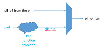
I need a MUX to switch the clock between normal mode and test mode. So, I don't care about any transient state when clock switching. Under the case(1), 'pll_c4_sw' is the switched output clock. Some IP use 'pll_c4_sw' this clock. 'pll_c4' is the clock from PLL under test mode when the 'sel' signal is 1. 'clk_pin' is the input clock from other device via normal FPGA pin and pin function selection function (combinational circuit) when the 'sel' signal is 0.
Unfortunately, Quartus13.1 tell me that "PLL "pll|altpll_component|auto_generated|pll1" has parameters clk4_multiply_by and clk4_divide_by specified but port CLK[4] is not connected." when I use the Stratix III device under the case(1).
Do you have any idea about this case? If you have some idea, could you please tell me? Thank you very much.
Case(1):
assign pll_c4_sw = sel? pll_c4 : clk_pin;
- Mark as New
- Bookmark
- Subscribe
- Mute
- Subscribe to RSS Feed
- Permalink
- Report Inappropriate Content
Sorry for the late response. Did you try using the ALTCLKCTRL block. It helps in clock switching.
This thread will be transitioned to community support. If you have a new question, feel free to open a new thread to get the support from Intel experts. Otherwise, the community users will continue to help you on this thread. Thank you
- Subscribe to RSS Feed
- Mark Topic as New
- Mark Topic as Read
- Float this Topic for Current User
- Bookmark
- Subscribe
- Printer Friendly Page

