- Mark as New
- Bookmark
- Subscribe
- Mute
- Subscribe to RSS Feed
- Permalink
- Report Inappropriate Content
Hello, Intel expert,
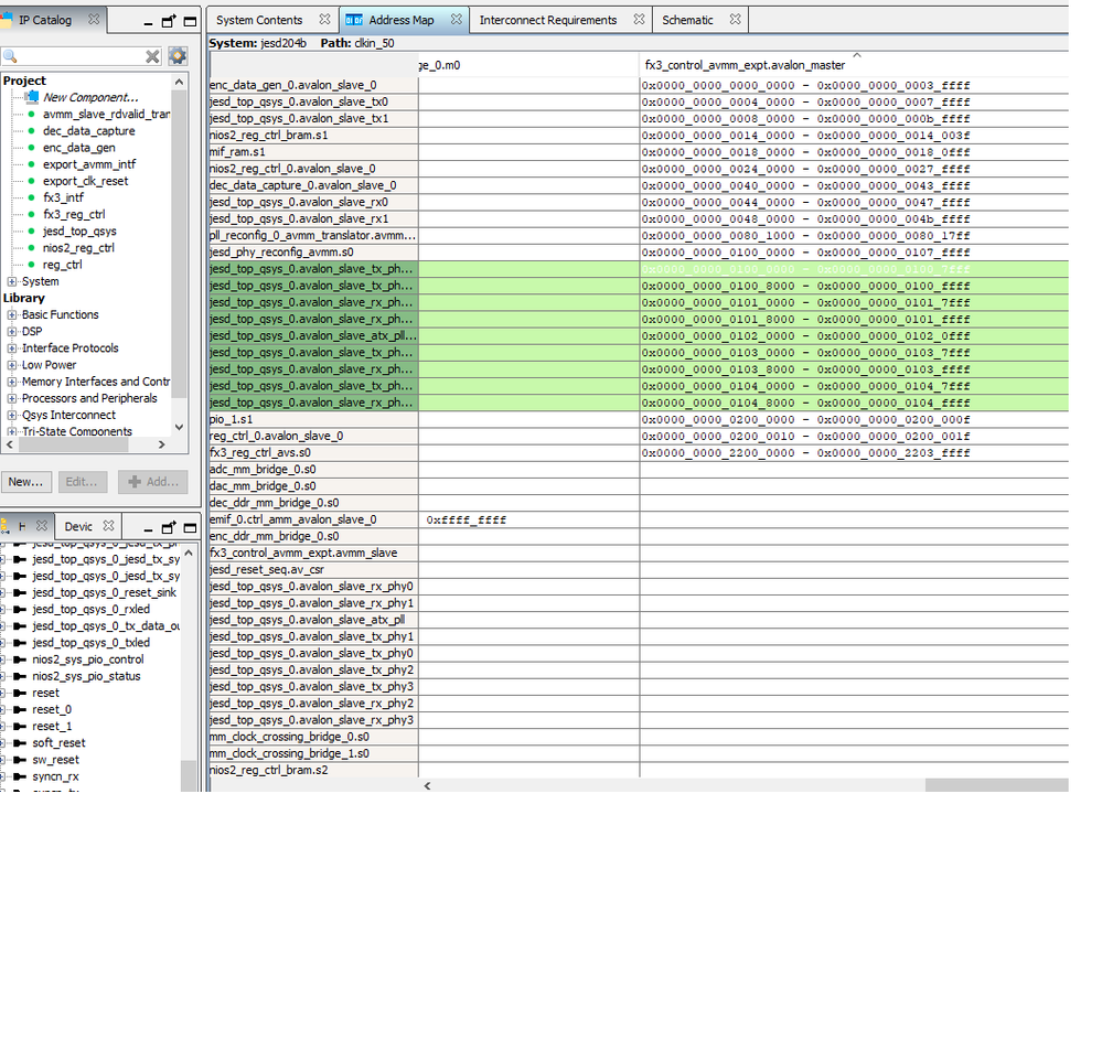
I have a very basic question here. while I start working on a TI JESD204B project, I have to figure out how the FX3(USB module) configured the FPGA device. have a look at the attached address map, from FX3 Master will control a lot of salves through the memory map. I assume the FX3 master send out contents to a slave through the assigned space, but I have tracking the signal link from the Master write command to the slave receiver. I tried several times, but I couldn't find or figure out how the memory address on the bus was decoded and distributed.
I am pretty new to the Avalon architecture, could anyone familiar Avalon bus give me some hint, link that explain how the Avalon master and slave arrange the memory space, where the address decode happened.
Thanks
David
Link Copied
- Mark as New
- Bookmark
- Subscribe
- Mute
- Subscribe to RSS Feed
- Permalink
- Report Inappropriate Content
I'm not sure what your question actually is, but the host (master) issues read and write commands to the Platform Designer interconnect, which then sends them to the appropriate agent (slave) address location. All of these agents are in the host's address space.
The Avalon spec is here: https://www.intel.com/content/dam/altera-www/global/en_US/pdfs/literature/manual/mnl_avalon_spec.pdf
- Mark as New
- Bookmark
- Subscribe
- Mute
- Subscribe to RSS Feed
- Permalink
- Report Inappropriate Content
- Mark as New
- Bookmark
- Subscribe
- Mute
- Subscribe to RSS Feed
- Permalink
- Report Inappropriate Content
I am new and learning, hope get some help to save time and move fast. I should have read the manual carefully and patiently. I will figure out what I want to know.
Thank you for asking.
David
- Subscribe to RSS Feed
- Mark Topic as New
- Mark Topic as Read
- Float this Topic for Current User
- Bookmark
- Subscribe
- Printer Friendly Page
