- Mark as New
- Bookmark
- Subscribe
- Mute
- Subscribe to RSS Feed
- Permalink
- Report Inappropriate Content
I can see from this thread that a differential (LVDS) EMIF PLL reference clock is only supported in LVDS I/O banks (and not 3 V I/O banks) in Arria 10:
https://community.intel.com/t5/Programmable-Devices/Is-LVDS-supported-on-the-dedicated-clock-input-of-the-Cyclone-10/td-p/270112
However, synthesis fails even if I follow this rule for the EMIF's "address and command bank", but try to use a 3 V I/O bank for the EMIF's "data bank":
This error occurs even after I have stripped down my pin assignments to the absolute minimum. I only constrain the LVDS PLL reference clock to be in Bank 2K (which is an LVDS bank) and I constrain just one data bit to be in Bank 2L (which is a 3 V I/O bank). No other pin constraints are defined:
I have carefully followed the "I/O Bank Usage" guidelines on p. 17 of "External Memory Interfaces Intel Arria 10 FPGA IP User Guide):
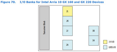
I have carefully checked the I/O bank types on p. 105 of "Intel Arria 10 Core Fabric and General Purpose I/Os Handbook":
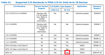
I have carefully checked Table 33 on p. 101 of the same document, which indicates that SSTL-15 should be supported in 3 V I/O banks:
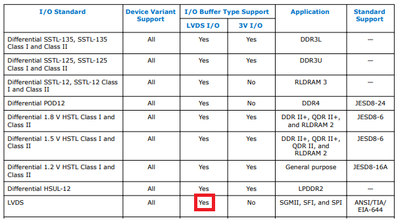
And, on p. 102, LVDS should be supported in LVDS I/O banks:
Therefore, I don't understand why this doesn't work.
As a first sanity check, I have confirmed that constraining the data pins to be in I/O Bank 2J (an LVDS bank) synthesizes without error:
What am I missing here? Is there some way to avoid this synthesis error?
- Mark as New
- Bookmark
- Subscribe
- Mute
- Subscribe to RSS Feed
- Permalink
- Report Inappropriate Content
@AdzimZM_Intel My understanding from the documentation is that disabling all the on-chip termination damages performance.
Since it is so difficult to get clear and reliable information from Intel (and so much time has already been wasted in this pursuit), we decided to redesign our hardware to use a single-ended reference clock.
Link Copied
- Mark as New
- Bookmark
- Subscribe
- Mute
- Subscribe to RSS Feed
- Permalink
- Report Inappropriate Content
Are you using Standard or Pro? If you're using Pro, you could try using Interface Planner.
Also, what happens if you remove the pin assignments for the memory from the Pin Planner and just let the Fitter try a placement? You could still make a single assignment, like for CK0, to select the address/command bank, an assignment for the reference clock, one for RZQ, and each of the DQS signals. The Fitter could then select valid locations for the DQ. Use the Read Me from the IP generation as a guide.
- Mark as New
- Bookmark
- Subscribe
- Mute
- Subscribe to RSS Feed
- Permalink
- Report Inappropriate Content
@sstrell I am using Quartus 21.3 Pro. I tried using the Interface Planner for a couple of hours, but I couldn't really see how to use the tool effectively. In the end, it just seemed easier to edit pin assignments in the Pin Planner, then compile the design. Did I miss a useful feature of the Interface Planner?
I tried many variations of constraining different pin assignments. With no pin assignments at all, the design builds without error. My key requirement is that I would like data pins to be in Bank 2L, but any attempt to do that causes an error. Actually, the differential clock could be a red herring - I'm now seeing that this constraint alone causes the fitter to fail:
So maybe it is simply the case that the EMIF's data bank must be an LVDS I/O bank? I didn't find any suggestion of this in the documentation.
I will try the combinations of pin assignments you suggested, but I feel quite sure I already tried something very similar without success.
- Mark as New
- Bookmark
- Subscribe
- Mute
- Subscribe to RSS Feed
- Permalink
- Report Inappropriate Content
Hi Herry,
Thanks for using Intel Community.
I will assist you to debug this error.
It's great if you can share a simple design that can reproduce the error.
Do you check the IO banks used whether they are adjacent to each other or not?
Thanks & Regards,
Adzim
- Mark as New
- Bookmark
- Subscribe
- Mute
- Subscribe to RSS Feed
- Permalink
- Report Inappropriate Content
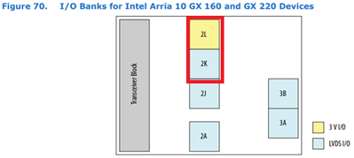
@AdzimZM_Intel I am trying to use Bank 2L and Bank 2K. As far as I understand, they are "adjacent" because they are next to each other in this diagram:
I have attached a minimal project (Quartus 21.3 Pro), containing only the EMIF. This reproduces the error:
There is only 1 pin assignment. If I remove this, then the project builds without error:
- Mark as New
- Bookmark
- Subscribe
- Mute
- Subscribe to RSS Feed
- Permalink
- Report Inappropriate Content
@AdzimZM_Intel Have you looked at the project I attached for you? Can you offer any advice?
- Mark as New
- Bookmark
- Subscribe
- Mute
- Subscribe to RSS Feed
- Permalink
- Report Inappropriate Content
Check out this training, which will explain how Interface Planner will make this super easy to fix:
- Mark as New
- Bookmark
- Subscribe
- Mute
- Subscribe to RSS Feed
- Permalink
- Report Inappropriate Content
@sstrell Thank you - there were 2 key features I missed:
- This mysterious button lists all legal placement options for a pin:
.
- This button places all pins that only have 1 legal location remaining:
.
This allowed me to confirm quite quickly that Quartus forbids the use of Bank 2L in a DDR3 interface that uses an LVDS PLL reference clock. It's not automatic by any means, but by process of elimination I was able to find that all "legal" locations turned out to be illegal.
It's a shame this doesn't appear to be documented anywhere, as I would be interested to know why this is forbidden.
- Mark as New
- Bookmark
- Subscribe
- Mute
- Subscribe to RSS Feed
- Permalink
- Report Inappropriate Content
Hello Herry,
I think the I/O Bank 2L which is the 3V I/O bank is not supports the termination.
You can refer to section 5.1 on page 100 of " Intel Arria 10 Core Fabric and General Purpose I/Os Handbook".
I think that is the main reason on why you cannot make the DQ pin placement in the Bank 2L.
Regards,
Adzim
- Mark as New
- Bookmark
- Subscribe
- Mute
- Subscribe to RSS Feed
- Permalink
- Report Inappropriate Content
@AdzimZM_Intel I'm not sure which part of that section you are referring to exactly. Are you referring to the part that says that single-ended I/O in 3 V I/O banks don't support "RD on-chip termination (OCT)"?
How do I know which single-ended I/O in my design needs "OCT"?
- Mark as New
- Bookmark
- Subscribe
- Mute
- Subscribe to RSS Feed
- Permalink
- Report Inappropriate Content
As I mentioned earlier, look at the Read Me generated by the IP to see the pin layout for the fixed pins required, like OCT.
- Mark as New
- Bookmark
- Subscribe
- Mute
- Subscribe to RSS Feed
- Permalink
- Report Inappropriate Content
Hi Herry,
Your DQ and DQS signals should required the termination right.
If you make the termination assignment for the DQS or DQ signals, the Quartus will show the error like below.
The 3V I/O bank does not support the internal Vref generation which I think that the DQ for DDR3 required the Vref.
Maybe Bank 2L is not suitable for the DQ signal and you should use other I/O bank for this signal.
Thanks,
Adzim
- Mark as New
- Bookmark
- Subscribe
- Mute
- Subscribe to RSS Feed
- Permalink
- Report Inappropriate Content
Hi Harry,
May I know any update or feedback regarding to this topic?
Thanks,
Adzim
- Mark as New
- Bookmark
- Subscribe
- Mute
- Subscribe to RSS Feed
- Permalink
- Report Inappropriate Content
@AdzimZM_Intel I did not understand your previous message. I could not see any problem related to termination. It seems like you tried to attach an image, but it failed:
Could you please re-send this image?
- Mark as New
- Bookmark
- Subscribe
- Mute
- Subscribe to RSS Feed
- Permalink
- Report Inappropriate Content
Hi Harry,
When you want to use the 3V I/O bank, you need to disable the calibrated OCT for A/C signals, CLK signals and DQ signals.
After you changed the setting in the EMIF IP, make sure that you regenerate the IP.
Regards,
Adzim
- Mark as New
- Bookmark
- Subscribe
- Mute
- Subscribe to RSS Feed
- Permalink
- Report Inappropriate Content
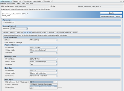
@AdzimZM_Intel How do I do that? The only option I can see related to on-chip termination in the EMIF IP is in FPGA I/O -> PHY Inputs:
Choosing either "LVDS with On-Chip Termination" or "LVDS without On-Chip Termination" seems to make no difference at all. The build still fails with the same errors.
I sent you my project in a previous post, so you can confirm this yourself if you want.
- Mark as New
- Bookmark
- Subscribe
- Mute
- Subscribe to RSS Feed
- Permalink
- Report Inappropriate Content
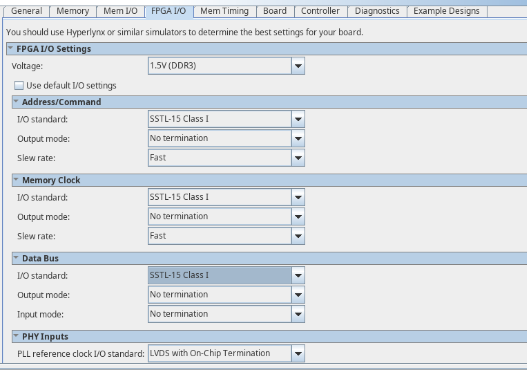
You can do that by setting "No termination" to the FPGA I/O setting.
- Address/Commands
- Output Mode = No Termination
- Memory Clock
- Output Mode = No Termination
- Data Bus
- Output Mode = No Termination
- Input Mode = No Termination
- Mark as New
- Bookmark
- Subscribe
- Mute
- Subscribe to RSS Feed
- Permalink
- Report Inappropriate Content
- Mark as New
- Bookmark
- Subscribe
- Mute
- Subscribe to RSS Feed
- Permalink
- Report Inappropriate Content
@AdzimZM_Intel This doesn't seem to change anything. Termination works fine with a single-ended PLL reference clock... and the fitter still fails with an LVDS reference clock, even if I disable termination.
Therefore, the problem does not seem to be related to this termination.
I sent you my project in a previous post, so you could have checked this.
- Mark as New
- Bookmark
- Subscribe
- Mute
- Subscribe to RSS Feed
- Permalink
- Report Inappropriate Content
Hi @hcom,
Coping from A10 EMIF handbook
I/O Banks Selection
• For each memory interface, select consecutive I/O banks.
• A memory interface can only span across I/O banks in the same I/O column.
• Because I/O bank 2A is also employed for configuration-related operations, you
can use it to construct external memory interfaces only when the following
conditions are met:
— The pins required for configuration related use (such as configuration bus for
Fast Passive Parallel mode or control signals for Partial Reconfiguration) are
never shared with pins selected for EMIF use, even after configuration is
complete.
— The I/O voltages are compatible.
— The design has achieved a successful fit in the Intel Quartus Prime software.
Refer to the Intel Arria 10 Device Handbook and the Configuration Function
column of the Pin-Out files for more information about pins and configuration
modes.
• The number of I/O banks that you require depends on the memory interface
width.
• The 3V I/O bank does not support dynamic OCT or calibrated OCT. To place a
memory interface in a 3V I/O bank, ensure that calibrated OCT is disabled for the
address/command signals, the memory clock signals, and the data bus signals,
during IP generation.
• In some device packages, the number of I/O pins in some LVDS I/O banks is less
that 48 pins.
Changing the termination will allow you to place in the 3V I/O bank.
I'm not able to do it in your design as the changes in the IP need to be regenerate and the top level file has missing port.
Then I create the example design by following your IP configuration.
The change is working from my side.
You may test the design that I've attached.
Thank you.
Adzim
- Mark as New
- Bookmark
- Subscribe
- Mute
- Subscribe to RSS Feed
- Permalink
- Report Inappropriate Content
@AdzimZM_Intel For some reason, if I try to make the changes in my project, it still doesn't work.
Could you explain a bit about the project you attached? There seem to be a lot of files in there that are not used. Is that correct? Why is this project totally different from my project? It's very difficult for me to find what is the difference when you create a new project from scratch. Could you just make the necessary change in the project I sent? Wouldn't this be the quickest solution for both of us?
- Subscribe to RSS Feed
- Mark Topic as New
- Mark Topic as Read
- Float this Topic for Current User
- Bookmark
- Subscribe
- Printer Friendly Page


