- Mark as New
- Bookmark
- Subscribe
- Mute
- Subscribe to RSS Feed
- Permalink
- Report Inappropriate Content
I didn't get the line in EMIF IP manual "Ensure that the pins of a single external memory interface reside within a single I/O column." Please explain..
Link Copied
- Mark as New
- Bookmark
- Subscribe
- Mute
- Subscribe to RSS Feed
- Permalink
- Report Inappropriate Content
I/O in S10 are arranged in columns which are organized into banks, which are in turn organized into 12-pin I/O lanes. You use one or more banks to implement an EMIF, but you want those banks to all be in the same I/O column in order to meet timing and make sure the interface works. You can have multiple memory interfaces in the same column (which in some cases allows you to share resources to implement the multiple interfaces), but you can't have a single interface span multiple columns.
See this online training for an overview of the EMIF architecture and implementation:
https://www.intel.com/content/www/us/en/programmable/support/training/course/omem1121.html
#iwork4intel
- Mark as New
- Bookmark
- Subscribe
- Mute
- Subscribe to RSS Feed
- Permalink
- Report Inappropriate Content
I have attached a file which has banks partition and these banks are not in single column. need some more explaination
THANKS AND REGARDS for replying to the previous mail.
- Mark as New
- Bookmark
- Subscribe
- Mute
- Subscribe to RSS Feed
- Permalink
- Report Inappropriate Content
As S10 is devided into 3 i/o lanes, I wanted to know how these i/o lanes are divided in s10.
- Mark as New
- Bookmark
- Subscribe
- Mute
- Subscribe to RSS Feed
- Permalink
- Report Inappropriate Content
- Mark as New
- Bookmark
- Subscribe
- Mute
- Subscribe to RSS Feed
- Permalink
- Report Inappropriate Content
The I/O columns are how they're organized on the chip die. They're not a 1-to-1 match with the pins.
#iwork4intel
- Mark as New
- Bookmark
- Subscribe
- Mute
- Subscribe to RSS Feed
- Permalink
- Report Inappropriate Content
Hi @hb0001 ,
I think @sstrell have a point. 😊
This is just for your additional reference, you may refer to section "3.1.2. Intel Stratix 10 EMIF Architecture: I/O Column" in this UG , refer to Figure 3 for architecture of Stratix 10 I/O Column.
UG link--> https://www.intel.com/content/dam/www/programmable/us/en/pdfs/literature/hb/stratix-10/ug-s10-emi.pdf
Hope this helps.
Thanks
Regards,
Aida
- Mark as New
- Bookmark
- Subscribe
- Mute
- Subscribe to RSS Feed
- Permalink
- Report Inappropriate Content
ok, thank you so much.
Which banks do you recommend to interface parallel nor flash.
it will be a great help if you tell how many banks do we need to interface parallel nor flash 512Mb .
Thank you in advance.
- Mark as New
- Bookmark
- Subscribe
- Mute
- Subscribe to RSS Feed
- Permalink
- Report Inappropriate Content
Hi @hb0001 ,
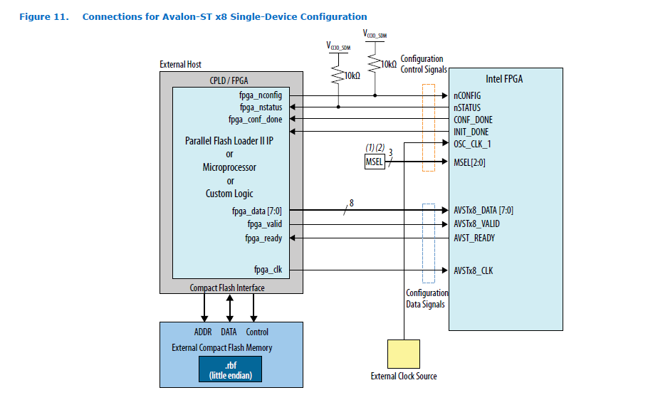
If I understand correctly, you are referring to below PFL IP. The bank is varies depend on the device's OPN. You need to connect it using dedicated config pins (example shown in Figure below) . For more details , you may checkout this Stratix 10 UG (start from page 40) --> https://www.intel.com/content/dam/www/programmable/us/en/pdfs/literature/hb/stratix-10/ug-s10-config.pdf#page=40&zoom=100,0,0
In Table 2 of the pin connection guideline handbook, there is a list of this dedicated config pins. You can check this config pins located at which bank number in the Intel FPGA Pin-out file. Kindly refer to link provided below.
Pin Connection Guideline --> https://www.intel.com/content/dam/www/programmable/us/en/pdfs/literature/dp/stratix-10/pcg-01020.pdf
Pin-out file for Intel FPGAs--> https://www.intel.com/content/www/us/en/programmable/support/literature/lit-dp.html
Regards,
Aida
- Subscribe to RSS Feed
- Mark Topic as New
- Mark Topic as Read
- Float this Topic for Current User
- Bookmark
- Subscribe
- Printer Friendly Page
