- 신규로 표시
- 북마크
- 구독
- 소거
- RSS 피드 구독
- 강조
- 인쇄
- 부적절한 컨텐트 신고
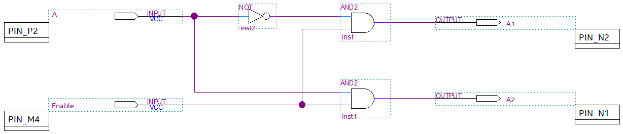
Intel Community, I recently purchased the Max V Development Kit. I figured out how to use the Quartus Prime Lite and successfully installed the Blaster. Created a simple encoder logic circuit, two inputs, one as a 0 or 1 input and the other an enable input. The circuit comprises of two 'AND' gates and on 'NOT' gate. When the first input is low the first AND gate input is low and the other AND input is high because of the NOT gate. The second input is an enabling input which allow the true states of the AND gates to be outputted else the outputs are always low when the enable input is low. Successfully created this logic, manually assigned pins, compiled and synthesized, etc. Successfully downloaded to the Max V kit. Wired up to test the CPLD, nothing. Absolutely nothing. I am not sure how to wire the board for the inputs to be applied. I assigned J6.1 as input, J6.2 as enable input. Pins J6.9 and J6.10 are the two AND gate outputs. Also, I accepted the 3.3 LV default. When I test with external switches to the board and outputs to a O-scope, nothing. I have searched for weeks any examples on interfacing external inputs devices and output devices to the board and have not found any thing. Is there any help to be found in the Intel Community? Thank you. My email is : moejjunior@gmail.com
Please note that I originally posted this last month with no reply. Frustrating.
링크가 복사됨
- 신규로 표시
- 북마크
- 구독
- 소거
- RSS 피드 구독
- 강조
- 인쇄
- 부적절한 컨텐트 신고
Hello,
I apologize for your unpleasant experience from your old post. I will try my best to help you.
Do you receive any kind of errors in your design? If yes, what are the errors?
I would advise you to look for blink tutorial on Youtube and see if your FPGA can work that. Please let me know if it works.
Thank you.
- 신규로 표시
- 북마크
- 구독
- 소거
- RSS 피드 구독
- 강조
- 인쇄
- 부적절한 컨텐트 신고
Hello,
>> I apologize for your unpleasant experience from your old post. I will try my best to help you.
Thank you.
>> Do you receive any kind of errors in your design? If yes, what are the errors?
No errors, some warnings only.
>> I would advise you to look for blink tutorial on Youtube and see if your FPGA can work that. Please let me know if it works.
I am using the Max V CPLD Develpment Kit, no FPGA is on the board.
- 신규로 표시
- 북마크
- 구독
- 소거
- RSS 피드 구독
- 강조
- 인쇄
- 부적절한 컨텐트 신고
Assuming I have the right board, J6.9 and J6.10 are incorrect for N1 and N2. N1 and N2 are on J6.6 and J6.5 respectively. See page 2-8 here:
- 신규로 표시
- 북마크
- 구독
- 소거
- RSS 피드 구독
- 강조
- 인쇄
- 부적절한 컨텐트 신고
Hell sstrell,
You have the right board.
>> Assuming I have the right board, J6.9 and J6.10 are incorrect for N1 and N2. N1 and N2 are on J6.6 and J6.5 respectively.
Pins J6.9 and J6.10 are the two AND gate outputs. Also, I accepted the 3.3 LV default. When I test with external switches to the board and outputs to a O-scope, nothing. See attached pictures.
Am I to have additional pins connected. If I am using 3.3 LV, what must be done with the other power level pins?
Thank you.
- 신규로 표시
- 북마크
- 구독
- 소거
- RSS 피드 구독
- 강조
- 인쇄
- 부적절한 컨텐트 신고
As I stated, N1 and N2 are the MAX V device pin names, but they are actually connected to J6.6 and J6.5, not J6.9 and J6.10. Attach your scope to the correct pins to see the outpu.
- 신규로 표시
- 북마크
- 구독
- 소거
- RSS 피드 구독
- 강조
- 인쇄
- 부적절한 컨텐트 신고
We do not receive any response from you to the previous question/reply/answer that I have provided. This thread will be transitioned to community support. If you have a new question, feel free to open a new thread to get the support from Intel experts. Otherwise, the community users will continue to help you on this thread. Thank you.
- 신규로 표시
- 북마크
- 구독
- 소거
- RSS 피드 구독
- 강조
- 인쇄
- 부적절한 컨텐트 신고
AminT_Intel,
I been away on travel. Still on this project, no success.
I am still having problems. A PDF file is provided. The logic circuit is simple. Board not working the way expected.
Thank you.
- 신규로 표시
- 북마크
- 구독
- 소거
- RSS 피드 구독
- 강조
- 인쇄
- 부적절한 컨텐트 신고
AminT_Intel
I still need help. See my recent reply.
Thank you.
- 신규로 표시
- 북마크
- 구독
- 소거
- RSS 피드 구독
- 강조
- 인쇄
- 부적절한 컨텐트 신고
Hello sstrell,
I been away on work travel. Still on this project, no success.
I am still having problems. A PDF file is provided. The logic circuit is simple. Board not working the way expected.
Thank you.