- Als neu kennzeichnen
- Lesezeichen
- Abonnieren
- Stummschalten
- RSS-Feed abonnieren
- Kennzeichnen
- Anstößigen Inhalt melden
Hello,
I have a design with a custom QSPI communication link between a TI DSP processor and a MAX 10 FPGA. The design was tested to work consistently with valid data exchange when the FPGA code is compiled using Quartus Prime Lite v15.1.0.
We purchased the Intel Functional Safety Data Package and so we would like to migrate to Quartus Prime Lite v17.0.2, since it is the latest qualified version for the FSDP. We would eventually move to Quartus Prime Standard v17.0.2 once we need the extra logic lock and partition features for functional safety, but for now we are using the Lite edition.
But when we compile with v17.0.2, the QSPI data exchange no longer works and we get intermittent bad data. We also tried an earlier working commit of our code that used standard SPI instead of QSPI and the same thing happened where it worked with 15.1.0, but not 17.0.2.
Is there some Quartus default setting that I need to change to make the compilation results more similar to what I get with v15.1.0?
I've attached the project .qsf file which remains the same whether I compile with v15.1.0 or v17.0.2, as well as the project .qdf file which was generated when I compiled with v17.0.2.
When I compare the assignment_defaults.qdf file from the Quartus 17.0.2 installation directory with the one generated by 17.0.2 in the project, there are only a couple of lines that are different:
Default settings:
set_global_assignment -name OCP_HW_EVAL Enable
set_global_assignment -name EDA_EXTRA_ELAB_OPTION "\"\"" -section_id ?
Project .qdf setting:
set_global_assignment -name OCP_HW_EVAL -value OFF
(the EDA_EXTRA_ELAB_OPTION line from the default is missing in the project .qdf, so I'm assuming the default in the installation directory is being used?)
Are there any important settings that I would need to change to make the compilation more similar?
I'm a bit of a beginner, so any help would be appreciated.
Thanks,
Udell
Link kopiert
- Als neu kennzeichnen
- Lesezeichen
- Abonnieren
- Stummschalten
- RSS-Feed abonnieren
- Kennzeichnen
- Anstößigen Inhalt melden
Your project file references a timing constraint file (andromeda.sdc) but you don't include it.
Do your designs compile AND MEET TIMING under both versions of Quartus?
How much slack is there in the worst case timing path(s)?
Are your clocks correctly constrained?
- Als neu kennzeichnen
- Lesezeichen
- Abonnieren
- Stummschalten
- RSS-Feed abonnieren
- Kennzeichnen
- Anstößigen Inhalt melden
Hi ak6dn,
Thanks for your response.
I can't provide the .sdc as it was written by a contracted 3rd party and there may be some intellectual property issues. The compilation reports said all timing constraints were met for both versions.
I've attached the sta reports if you want to look at them, but here is a worst-case summary from the sta report:
Slow 1200mv 100C model
- setup slack:
- v15.1.0: 0.273
- v17.0.2: 0.250
- hold slack:
- v15.1.0: 0.256
- v17.0.2: 0.282
- recovery slack:
- v15.1.0: 1.974
- v17.0.2: 2.176
- removal slack:
- v15.1.0: 0.932
- v17.0.2: 0.710
- min. pulse width slack:
- v15.1.0: 3.434
- v17.0.2: 3.434
Slow 1200mv -40C model
- setup slack:
- v15.1.0: 0.412
- v17.0.2: 0.356
- hold slack:
- v15.1.0: 0.250
- v17.0.2: 0.281
- recovery slack:
- v15.1.0: 2.123
- v17.0.2: 2.276
- removal slack:
- v15.1.0: 0.833
- v17.0.2: 0.624
- min. pulse width slack:
- v15.1.0: 3.434
- v17.0.2: 3.434
Fast 1200mv -40C model
- setup slack:
- v15.1.0: 0.454
- v17.0.2: 0.585
- hold slack:
- v15.1.0: 0.097
- v17.0.2: 0.110
- recovery slack:
- v15.1.0: 3.488
- v17.0.2: 3.564
- removal slack:
- v15.1.0: 0.389
- v17.0.2: 0.292
- min. pulse width slack:
- v15.1.0: 0
- v17.0.2: 0
I would have thought if timing constraints were met in both cases, it would work with either version of Quartus. Also, all inputs and outputs between the SPI/QSPI module and top level ports are registered.
One thing I noticed, in the .sdc file, the QSPI ports all have set_false_path and there's a note from the 3rd party who wrote it, that this was done since all inputs are synchronized with 2x registers to the 100MHz clock (which I've confirmed in the source code).
Some extra background is the original standard SPI version of the code was developed by 3rd party FPGA experts. Then I modified the SPI to have a QSPI read mode as well. Both versions work when compiled with v15.1.0, but don't work when compiled with v17.0.2.
Thanks for your help.
- Als neu kennzeichnen
- Lesezeichen
- Abonnieren
- Stummschalten
- RSS-Feed abonnieren
- Kennzeichnen
- Anstößigen Inhalt melden
Several comments:
SET_FALSE_PATH is going to remove any timing constraints on those paths from the referenced clock. So you won't know of those paths are failing as they aren't checked. Be careful with using that directive.
Do both SPI and QSPI modes fail in the v17 compiled version? Or just QSPI?
The timing values in the reports for v15 vs v17 are pretty close, so it looks like nothing is wildly off.
Which generated clock is the SPI logic working off?
- Als neu kennzeichnen
- Lesezeichen
- Abonnieren
- Stummschalten
- RSS-Feed abonnieren
- Kennzeichnen
- Anstößigen Inhalt melden
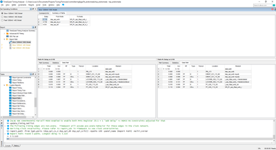
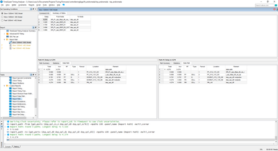
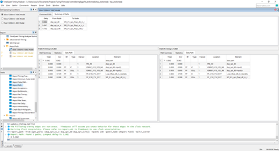
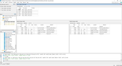
If I use TimeQuest and do a "Report Path" with -from and -to for all the SPI input and output ports at the toplevel, this is what I get:
For v15.1.0:
-from
-to
For v17.0.2:
-from
-to
From the timing reports of the paths, the slack seems like it's not too bad for the 10ns clock period. I don't quite get why even though the SET_FALSE_PATH for those ports listed above are in the sdc, I can still get the timing reports of the paths. I need to learn how to do timing constraints properly still. I'm guessing it's not constrained, but resulted in the numbers above? Those are only the paths -from or -to the toplevel ports and the SPI module pins I believe. I can't seem to get proper reports for the paths -from / -to the pins in the SPI module itself.
Both SPI and QSPI modes fail with v17.0.2. When it fails, the DSP reads back bad data intermittently, whereas with v15.1.0 the data read back is always correct.
The SPI module is clocked from PLL[0] which is the 100MHz clock.
Does it make sense that the original 3rd party used SET_FALSE_PATH because they are using 2x synchronizers on the inputs clocked to the internal 100MHz system clock and not using the external SPI CLK as a clock in the FPGA?
The note in the .sdc states
# False paths, since the design treats the SPI inputs
# by the internal fast system clock (no use of SPI_CLK as a clock)
- Als neu kennzeichnen
- Lesezeichen
- Abonnieren
- Stummschalten
- RSS-Feed abonnieren
- Kennzeichnen
- Anstößigen Inhalt melden
Hi,
Since you have a timing clean report, the design should work as designed. You may check with the designer whether the false path constraint is applied to the intended path.
Thanks.
Best regards,
KhaiY
- Tags:
- Hi
- Als neu kennzeichnen
- Lesezeichen
- Abonnieren
- Stummschalten
- RSS-Feed abonnieren
- Kennzeichnen
- Anstößigen Inhalt melden
Hi KhaiY,
I'm just trying to understand since I'm a bit of a beginner.
Since the design does not use the SPI clock coming from the external processor as a "clock" in the FPGA and is synchronized using 2x flip flops clocked to the FPGA 100MHz system clock, is that a typical case when you would use set_false_path?
After the synchronizers, the SPI signals are used in synchronous logic to read and write data in internal DPRAM and internal registers with Avalon-MM interface. Does the STA still check the paths after the synchronizers to ensure logic transitions will meet the internal 100MHz clock even though set_false_path is set on the external ports that feed the internal 100MHz synchronized logic?
Also, in case the problem isn't due to the SDC settings, are there any Quartus settings between v15.1 and v17.0.2 that I should focus on? There's quite a lot of settings.
Thanks for your help.
Best Regards,
USo00
- Als neu kennzeichnen
- Lesezeichen
- Abonnieren
- Stummschalten
- RSS-Feed abonnieren
- Kennzeichnen
- Anstößigen Inhalt melden
Hi,
Is there any reason of using the internal 2x clock instead of the SPI clock from the source? Where and how the false path assignment is added? Can you share the design example?
Thanks
Best regards,
KhaiY
- Als neu kennzeichnen
- Lesezeichen
- Abonnieren
- Stummschalten
- RSS-Feed abonnieren
- Kennzeichnen
- Anstößigen Inhalt melden
Hi KhaiY,
I'm not sure of the original reasoning to use the 100MHz internal clock instead of the SPI 33MHz clock from the source, since it was written by a subcontracted 3rd party.
But, I think it is quite a common practice to do it this way to simply treat the SPI signals as asynchronous "signals" that are then sync'd to the FPGA clock through two (or more) series registers since the FPGA clock is faster.
Maybe there's just not enough margin going from the asynchronous external 33MHz SPI clock domain to the 100MHz FPGA system clock domain that slight differences between Quartus v15.1.0 and v17.0.2 would cause it to fail?
I guess an alternative way it could have been done is to use the external SPI clock as an actual "clock" signal in the FPGA and then use a dual-clocked FIFO for the clock-domain crossing to the 100MHz domain?
Here is an excerpt from the .sdc for the clocks and ports in question. These are the only constraints related to the SPI.
# ----------------------------------------
# ----------------------------------------
# EXT CLOCK & PLL
# ----------------------------------------
# ----------------------------------------

# External Clock Input
create_clock -name ext_clk25mhz -period 40.0 [ get_ports -nocase ext_clk25mhz ]


# PLL Constraints
derive_pll_clocks

# FPGA internal Uncertainties
derive_clock_uncertainty


# Defines the system clock : output of PLL
set sys_clk {i_pll|altpll_component|auto_generated|pll1|clk[0]}

# ----------------------------------------
# ----------------------------------------
# Set Clock Groups
# ----------------------------------------
# ----------------------------------------

set_clock_groups -asynchronous -group [ get_clocks ext_clk25mhz ]
set_clock_groups -asynchronous -group [ get_clocks $sys_clk ]

# ----------------------------------------
# ----------------------------------------
# SPI interface with DSP
# ----------------------------------------
# ----------------------------------------
# False paths, since the design treats the SPI inputs
# by the internal fast system clock (no use of SPI_CLK as a clock)
set_false_path -from [get_ports dsp_spi_cs_n]
set_false_path -from [get_ports dsp_spi_sclk]
set_false_path -from [get_ports dsp_spi_mosi]
set_false_path -to [get_ports dsp_spi_miso]
set_false_path -to [get_ports dsp_irq]
It's very concerning that updating to a newer version would cause the design to pass or fail.
Thanks for your help.
- Als neu kennzeichnen
- Lesezeichen
- Abonnieren
- Stummschalten
- RSS-Feed abonnieren
- Kennzeichnen
- Anstößigen Inhalt melden
Hi,
Can you remove the false path constraint applied to the data input to the FPGA and add an input/output delay to the input/output data port?
Thanks.
Best regards,
KhaiY
- Als neu kennzeichnen
- Lesezeichen
- Abonnieren
- Stummschalten
- RSS-Feed abonnieren
- Kennzeichnen
- Anstößigen Inhalt melden
Hi,
I'll have to figure out how to do that.
It still doesn't explain to me why the design works with Quartus v15.1.0, but not v17.0.2 though.
Best Regards,
Udell
- Als neu kennzeichnen
- Lesezeichen
- Abonnieren
- Stummschalten
- RSS-Feed abonnieren
- Kennzeichnen
- Anstößigen Inhalt melden
Hi,
The logic in the design is placed and routed differently every time you compile the design, which is why you will see different compilation result. Besides this, there are some bugs fixed and enhancement in the newer version of the software, this also the reason that you are seeing different compilation result.
Thanks.
Best regards,
KhaiY
- Als neu kennzeichnen
- Lesezeichen
- Abonnieren
- Stummschalten
- RSS-Feed abonnieren
- Kennzeichnen
- Anstößigen Inhalt melden
Thanks KhaiChein_Y_Intel,
I guess we'll have to tighten up the timing constraints then, so the different versions give more similar compilation results. Thanks for your help.
- Als neu kennzeichnen
- Lesezeichen
- Abonnieren
- Stummschalten
- RSS-Feed abonnieren
- Kennzeichnen
- Anstößigen Inhalt melden
Hi,
Since there is no other questions, I now transition this thread to community support. If you have a new question, feel free to open a new thread to get the support from Intel experts. Otherwise, the community users will continue to help you on this thread. Thank you.
Best regards,
KhaiY
- RSS-Feed abonnieren
- Thema als neu kennzeichnen
- Thema als gelesen kennzeichnen
- Diesen Thema für aktuellen Benutzer floaten
- Lesezeichen
- Abonnieren
- Drucker-Anzeigeseite


