- Mark as New
- Bookmark
- Subscribe
- Mute
- Subscribe to RSS Feed
- Permalink
- Report Inappropriate Content
Hi all,
I am working with SOM board with Arria 10 SX on it.
Signal Tap does not see differential clock signal from external freq generator. In the same time I see frequencies on external generator output pins (by oscilloscope).
Quartus 18.1 Pro. Compilation of project is finished successfully.
External clock generator (SI5338) prepares 2 frequencies: 125 MHz and 322.26 MHz as differential signals.
These signals connected to U24/U23 (REFCLK_GXBL1C_CHT_P) and W24/W23 (REFCLK_GXBL1C_CHB_P) pins.
I added some assignments in Assignment Editor regarding these signals (see attachment).
But FPGA project does not receive these signals.
I coded simple counter and instantiate it on each of frequencies: 100 MHz (USER_CLK from HPS), 125 MHz (from ext generator) and 322 MHz (from ext generator).
I see signal on output of counter (out signal pulse_out) on 100 MHz only. On the outputs pulse_out of 125 MHz and 322 MHz counters there is nothing.
*.sdc file includes:
# 125MHz for REFCLK_GXBL1C_CHT_P
create_clock -name CLK_125M -period 8 [get_ports REFCLK_GXBL1C_CHT_P]
# 322MHz for REFCLK_GXBL1C_CHB_P
create_clock -name CLK_322M -period 3.103 [get_ports REFCLK_GXBL1C_CHB_P]
Could you help me to understand what is the reason of this problem and what need to change to get right working FPGA?
Thank you in advance.
Dmitry
Link Copied
- Mark as New
- Bookmark
- Subscribe
- Mute
- Subscribe to RSS Feed
- Permalink
- Report Inappropriate Content
GXB transceiver are dedicated hardware and not part of the FPGA fabric. Their refclk input can't be tapped by Signaltap.
- Mark as New
- Bookmark
- Subscribe
- Mute
- Subscribe to RSS Feed
- Permalink
- Report Inappropriate Content
Hi, FvM
Thank you for reply.
I tapped not REFCLK input immediately, but output of counter which feed from REFCLK. Or does it not matter?
- Mark as New
- Bookmark
- Subscribe
- Mute
- Subscribe to RSS Feed
- Permalink
- Report Inappropriate Content
Let me know if there is any update from previous reply.
- Mark as New
- Bookmark
- Subscribe
- Mute
- Subscribe to RSS Feed
- Permalink
- Report Inappropriate Content
What are you using for your sampling clock? It would have to be faster than 322 MHz to accurately capture all 3 signals and I don't think Signal Tap supports a sampling clock that fast.
- Mark as New
- Bookmark
- Subscribe
- Mute
- Subscribe to RSS Feed
- Permalink
- Report Inappropriate Content
Hi, sstrell
Thank you for reply.
Perhaps I didn't explain the meaning of the question in sufficient detail.
As a sample clock, I use 100 MHz. The tap signal works at this frequency without question.
Additionally, I feed 2 frequencies (125 and 322 MHz) to the outer pins of the FPGA, which is higher than the clock sample of 100 MHz.
To make sure that the frequency data gets to the subsequent FPGA logic, I pass these frequencies through a divider counter with a divide factor of 120.
Accordingly, at the outputs of the dividers, I expect 125 MHz / 120 ~ 1 MHz and 322 MHz / 120 ~ 2.7 MHz. With both of these frequencies, the tap signal should cope without question.
The essence of my problem is that I see two input frequencies at the outputs of the external generator and on the pins of the FPGA, but I do not see them inside the FPGA using the Singal tap.
I'm not trying to see signals with a frequency of 322 MHz using a 100 MHz sample clock))
This is a debug circuit to confirm of receiving of input frequencies.
I also tried to pass the input frequencies through the PLL without frequency conversion as 1: 1, but with the subsequent division on the counter to lower it, but I also did not see the output frequency.
I apologize than the problem with FPGA pins configuration, but I am not sure.
Br, Dmitry
- Mark as New
- Bookmark
- Subscribe
- Mute
- Subscribe to RSS Feed
- Permalink
- Report Inappropriate Content
So you're trying to tap signals operating at about 1 MHz and about 2.7 MHz? Then you have the opposite problem of what I mentioned. The signals are so slow that they don't appear in the time seen in the capture buffer. What is your trigger condition? If you trigger on these divided signals themselves, you should be able to see them.
- Mark as New
- Bookmark
- Subscribe
- Mute
- Subscribe to RSS Feed
- Permalink
- Report Inappropriate Content
May I know if there is any update from previous reply?
- Mark as New
- Bookmark
- Subscribe
- Mute
- Subscribe to RSS Feed
- Permalink
- Report Inappropriate Content
Hi all who helped to me in this problem.
I will share the results that I found. Perhaps this will be useful to someone.
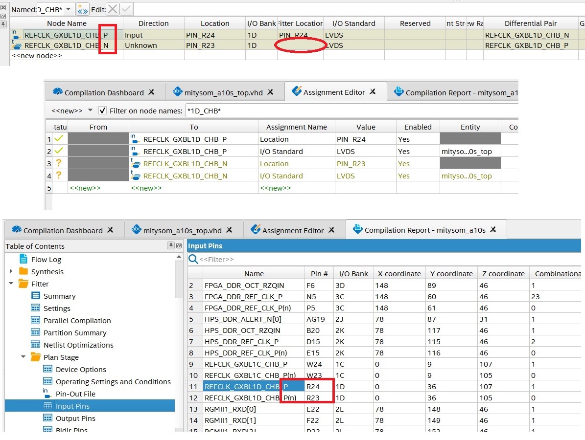
After first compilation the default FPGA project from GIT I see inconsistency between Pin Planner and Assignments from one side and results in Input Pins (Fitter report) on another side. You can see all that in attachments.
I think this result obviously do not allow to work the project in right manner.
It seems to me that this behavior is due to the fact that by default Quartus for signals of the LVDS type automatically creates a pair with the addition of "(n)" to the end of the name of the second signal. But by default, a pair of signals with the names "..._P" and "...N" is created in the project.
Unfortunately, Quartus' work with assignments is not a strong point. Changing assignments creates "garbage from old values" in assignment files, which have to be deleted manually (dancing with a tambourine).
After some effort, I cleaned out the assignment history and brought project into the desired state (After correction.jpg).
But this activity do not move me to desired result. (((
Faced with the need to manually intervene in editing the assignments, I'm not sure that I corrected the situation in full.
I decide to go by another way and stop the work with this FPGA project.
Thanks again everyone for the help.
Br, Dmitry.
- Subscribe to RSS Feed
- Mark Topic as New
- Mark Topic as Read
- Float this Topic for Current User
- Bookmark
- Subscribe
- Printer Friendly Page