- Mark as New
- Bookmark
- Subscribe
- Mute
- Subscribe to RSS Feed
- Permalink
- Report Inappropriate Content
In my design I deliberately designed two dual-port RAMs of single M9K block each, using them through both ports A and B in parallel.
I spent several days debugging the application I am designing failing in very strange way. Simulation and data captured from live system does not help to find the problem.
I started to dig into the deeps of Quartus reports (mostly out of desperation), and found that in fitter's RAM summary tab the location for both RAMs is the same (M9K_X15_Y19_N0) and that "Resource utilization per entity" list shows that one RAM is having 1 M9K assigned to it, and second does not!
Does it mean that Quartus "optimized" the design compacting two explicit memories into one physical memory?
This is technically fairly possible because I only use halves of these RAMs. However I can not understand how it can be done from interfacing point of view because I use ALL interfaces of both RAMs - are they time shared when combined?
How can I tell Quartus NOT to do it and leave separate M9K memories alone as they are designed?
Link Copied
- Mark as New
- Bookmark
- Subscribe
- Mute
- Subscribe to RSS Feed
- Permalink
- Report Inappropriate Content
Did you add the RAMs through code inference or by adding them as IP through the IP Catalog? If it was code inference, that might be the issue. If you show your code, that could help diagnose the problem.
Also, if you are using code inference, check out the templates in the Quartus text editor (Edit menu -> Insert Template) to make sure you are following the coding guidelines to have your design synthesized the way you intend.
- Mark as New
- Bookmark
- Subscribe
- Mute
- Subscribe to RSS Feed
- Permalink
- Report Inappropriate Content
Hello, thank you for your reply.
I used MegaWizard.
Code as simple as this:
reg [8:0] r_fir_RAM_address = {9{1'b0}};
wire [15:0] w_fir_RAM_data_out_lo;
wire [15:0] w_fir_RAM_data_out_hi;
reg [15:0] r_fir_RAM_data_in_lo = {16{1'b0}};
reg [15:0] r_fir_RAM_data_in_hi = {16{1'b0}};
reg r_fir_RAM_we = 1'b0;
fir_ram_lo fir_ram_lo (
.clock(FFCLK),
// address - same for both channels, even/odd
.address_a( { r_fir_RAM_address[8:0], 1'b0 } ),// even byte
.address_b( { r_fir_RAM_address[8:0], 1'b1 } ),// odd byte
// write enable
.wren_a(r_fir_RAM_we),
.wren_b(r_fir_RAM_we),
// indata
.data_a(r_fir_RAM_data_in_lo[7:0]),
.data_b(r_fir_RAM_data_in_lo[15:8]),
// outdata
.q_a(w_fir_RAM_data_out_lo[7:0]),
.q_b(w_fir_RAM_data_out_lo[15:8])
);
fir_ram_hi fir_ram_hi (
.clock(FFCLK),
// address - same for both channels, even/odd
.address_a( { r_fir_RAM_address[8:0], 1'b0 } ),// even byte
.address_b( { r_fir_RAM_address[8:0], 1'b1 } ),// odd byte
// write enable
.wren_a(r_fir_RAM_we),
.wren_b(r_fir_RAM_we),
// indata
.data_a(r_fir_RAM_data_in_hi[7:0]),
.data_b(r_fir_RAM_data_in_hi[15:8]),
// outdata
.q_a(w_fir_RAM_data_out_hi[7:0]),
.q_b(w_fir_RAM_data_out_hi[15:8])
);- Mark as New
- Bookmark
- Subscribe
- Mute
- Subscribe to RSS Feed
- Permalink
- Report Inappropriate Content
There seem to be a weak workaround (if it is a valid workaround at all) distributing the data across the whole M9K block. But there's a risk that at some stage Quartus (or its other version) identifies that design does not use specific addresses in the space, and pack everything as it wants and as it was not designed by the developer, causing problems and penalties in performance.
Thus I need explicit command/instruction for Quartus for NOT doing any RAM space optimizations, and leave M9K block and connections to it as designed in the project.
I am still not sure from previous replies if what I see is Quartus behavior as it was designed. I can not find any related information, articles, datasheets or whitepapers on the subject. The mechanism of this "optimization" is unclear as from my perspective it is, with current M9K block usage, simply impossible without any tricks or undocumented features.
Update: looked through, and played with all the options available in the "setting" section (compilation and fitting), which look like may affect the problem. No change. Nothing suitable in the "device" menus.
- Mark as New
- Bookmark
- Subscribe
- Mute
- Subscribe to RSS Feed
- Permalink
- Report Inappropriate Content
It seems Intel senior managers in customer support / application engineering had never used their portal as a customers.
1. It appears that these "Intel community forums" are the main support vehicle of the Intel. In my understanding community is a meeting place of the interested parties and people, who may know something, and be somehow responsible for something, and have some experience. "Community", as a term, is not a formal place to come and expect formal reliability and formal responsibility. See the definition of community here. IMHO, it is incorrect and misleading using word "community" as a buzzword for formal support services. What is service level agreement (SLA) of these forums? Where can I learn them in comprehensive way and set my expectation accordingly?
2. As it appeared that this community forum is formal customer support portal, I would expect to see real names of the Intel employees here, with their positions and locations, so that I know whom I am talking to. So far everyone I meet are nicknamed individuals with no indication what experience they have and if they are trustworthy or credible. Whatever "honored" profile holder is, I am not going to base my decision making on anonymous opinions if they do not convince me 100% and have no confirmation from other, trusted parties.
3. There seems to be another support means called "Intel customer support". I opened the ticket there, while filling the form there were no, absolutely no, questions/checkboxes what product issue I have so that ticket can be routed properly onto the respective team at the first place. There's only a "description" field to put custom information into. The form does not look like being customer-oriented, and makes an impression it is a support for people who do not have Intel web pages loading properly in their browser (webmaster support).
4. I had emails from "supportreplies", and these emails does not explicitly state that its mailbox is not monitored, and I had to learn it after writing several emails into there... so there's no way to give feedback to the support people privately without using this forum.
I was an HP IT resource center member for several years in the past (being an HP customer support expert employee), these days sometimes use support services and forums of Maxim Integrated, NXP, TI, Wiznet, Microchip and other component and IP vendors. I used Altera support services in the past - they were decent. As a customer, I rank the Intel support as the worst out of all in terms of the process. Yes, I am very small customer, but I expect to be guided through my problem resolution in expected, responsible and informed manner.
The support process is broken.
- Mark as New
- Bookmark
- Subscribe
- Mute
- Subscribe to RSS Feed
- Permalink
- Report Inappropriate Content
In reading your code snippet, for the instantiation of your two RAM blocks the **ONLY** difference is in the data input/output signals.
The address/data/control signals are IDENTICAL for each block.
So Quartus can easily (and validly) pack BOTH of your RAM blocks into a single M9K block that has a wide enough data port (of 32bits) and a deep enough depth (256 locations, as you indicate the upper address bit is always zero). 256*32 = 8192 < M9K size so it fits in one memory block.
Darn good optimization by Quartus. Why are you complaining?
- Mark as New
- Bookmark
- Subscribe
- Mute
- Subscribe to RSS Feed
- Permalink
- Report Inappropriate Content
Update: after some conversations we decided that it is not clear how to deal with the issue, and I decided to change architecture of the circuit using one single port RAM. It has performance penalty, but satisfies minimal requirements, thus there's no more urgency in and severity of dealing with the issue.
Special thanks to everyone who was involved into the escalation.
>Why are you complaining?
This is a very good question!
1. In my previous designs I have seen clear difference between performance of *8 and *16 M9K RAMs. I can not explain why *16 configuration is not up to speed, most probably it has some more logic involved speeding down the operation causing invalid data output at specific clock frequencies - I use ~112 MHz;
2. There must be an option to tell Quartus not to be that darn good, but perform as it was designed by the human designer. So far we did not find anything which would instruct Quartus to make 2 RAMs and not one RAM which (see my item #1) may not be up to speed causing artefacts in its output thus system failure;
3. The M9K guide for Cyclone 3, at its page 3-11, has a table listing possible configurations for True Dual Port RAM - the one I used in the design. Table 3-4 does not list 256*32 configuration. Thus Quartus must have had two RAMs. In general, the documentation does not show "native" configuration of the M9K blocks which provides maximum performance;
4. And finally, the actions and optimizations Quartus performing are not clear, and thus suspicious, without any traces in its warnings or informational messages. There must have been messages that Quartus merges RAMs, but there're none. Then only related are about Quartus rightfully reporting that MSBs of the addresses are not used.
- Mark as New
- Bookmark
- Subscribe
- Mute
- Subscribe to RSS Feed
- Permalink
- Report Inappropriate Content
Your code though is using SIMPLE dual port mode, so on page 3-9 table 3-3 applies.
256x32 is a valid configuration, thus Quartus did what it did.
- Mark as New
- Bookmark
- Subscribe
- Mute
- Subscribe to RSS Feed
- Permalink
- Report Inappropriate Content
"Quote ak6dn:
> Your code though is using SIMPLE dual port mode, so on page 3-9 table 3-3 applies. 256x32 is a valid configuration, thus Quartus did what it did."
This is real discovery for me. I use dual port RAMs in a way both ports can read from and write to same location at the same time. It does not happen often, but it may happen. Now I learn from you that what I do is "Simple dual-port mode supports simultaneous read and write operations to different locations".
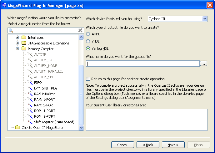
Let's see at the megawizard:
There's 2-port RAM, there're no "simple" or "true" in the list. I suspect something about RAM being "true" must be selected within 2-port RAM creation menu? Here're some more screenshots:
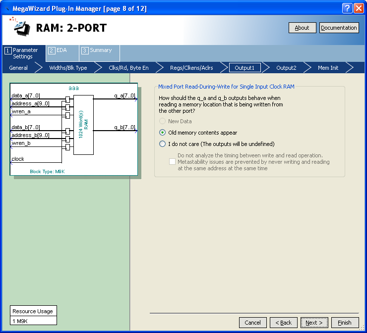
This screenshot assumes that what I create using wizard actually is able to read location being written to by another port. So what I make here can not be a simple RAM because simple RAM, per its definition in the document above is not able to read/write same location through different ports.
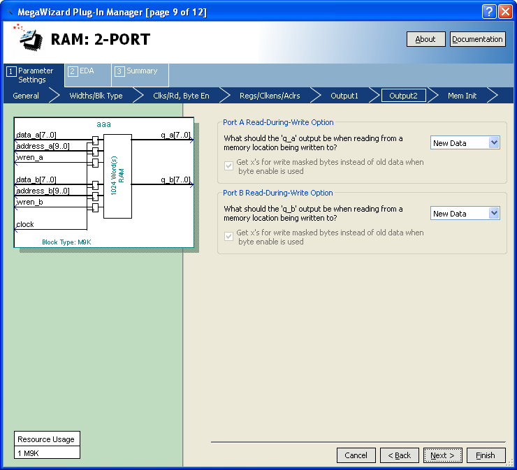
Next one confirms this:
This means that I can read location I am writing to, but does not explicitly say about what port to be used.
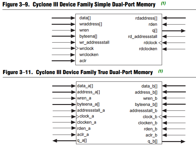
Let's compare the pictures in the document:
There're clear differences between simple and true dual ports; Looking at my previous replies to this thread I see there're signals defined corresponding to the true dual-port RAM, there're no "rdaddress" or "rden" signals... Do I miss anything?
Therefore, let's return to basics:
- do I understand properly that "simple" dual-port RAM does not support writing from port A and reading from port B at the same time? There's clear discrepancy in documentation and in what I see in Megawizard;
- Are you sure my RAM is simple dual port? How can I insert "True" dual port RAM into the project?
- Mark as New
- Bookmark
- Subscribe
- Mute
- Subscribe to RSS Feed
- Permalink
- Report Inappropriate Content
Hi Eugeny,
1. May I know what device you are targeting and Quartus version used?
2. I can see the code snippet provided, could you try to provide a design and achieve it here .qar. I will try to reproduce it at my end. You can email or private message me if it is confidential.
Thanks,
Regards
- Mark as New
- Bookmark
- Subscribe
- Mute
- Subscribe to RSS Feed
- Permalink
- Report Inappropriate Content
Hello, I am using Cyclone 3, Quartus versions tried are 12.0 SP2 and 13.0 SP1.
As a starting point I have put the definition of RAMs in one of my replies above, and briefly said how I used them. Putting code here is not appropriate as it is relatively big. The data being addressed through the address wires are in the first part of RAM, address MSb is always 0.
How can I send you a private message? Suspect that when I click your anonymous icon I must see something useful, but there's only progress indicator rotating.
Is your email address "SyafieqS_Intel@intel.com"? Who I am talking to?
- Mark as New
- Bookmark
- Subscribe
- Mute
- Subscribe to RSS Feed
- Permalink
- Report Inappropriate Content
Hi Eugeny,
Noted and glad to hear the issue had been addressed. Let me know if you have any other concern on this.
- Subscribe to RSS Feed
- Mark Topic as New
- Mark Topic as Read
- Float this Topic for Current User
- Bookmark
- Subscribe
- Printer Friendly Page
