- 신규로 표시
- 북마크
- 구독
- 소거
- RSS 피드 구독
- 강조
- 인쇄
- 부적절한 컨텐트 신고
Hello,
In my design, there is an asynchronous bus between FPGA and Microcontroller (Master). FPGA uses the edges on the signals WRN (Write active) and ALE (Address Enable) to classify if the signals on the bus indicate Data or Address .
As the logic is checking for the edges on WRN and ALE in a process, Quartus thinks they are clocks and gives timing errors: "WRN and ALE are clocks and they are not constrained".
How do I solve this issue having known that WRN and ALE are not clocks?
링크가 복사됨
- 신규로 표시
- 북마크
- 구독
- 소거
- RSS 피드 구독
- 강조
- 인쇄
- 부적절한 컨텐트 신고
Yes, I had set false paths on them. But Timing analyzer report still shows these two signals as unconstrained clocks in the clock status summary.
My Code:
--somewhere in the architecture
PROCESS ( ale, adbus )
BEGIN
IF ( ale'event AND ale = '0' ) THEN
address <= adbus;
END IF ;
END PROCESS;
PROCESS ( wrn, clearn, adbus )
BEGIN
IF clearn = '0' THEN
data<= "0000000000000000" ;
ELSIF ( wrn'event AND wrn = '1' ) THEN
data <= adbus( 15 DOWNTO 0 );
END IF ;
END PROCESS
I am using the edges of ALE and WRN to identify if it is address or data on the adbus, and the tool thinks these are clocks.
There are also warnings:
Warning (332060): Node: wrn was determined to be a clock but was found without an associated clock assignment.
Warning (332060): Node: ale was determined to be a clock but was found without an associated clock assignment.
- 신규로 표시
- 북마크
- 구독
- 소거
- RSS 피드 구독
- 강조
- 인쇄
- 부적절한 컨텐트 신고
The false path constraints are as follows:
set_false_path -from [get_ports WRN]
set_false_path -from [get_ports ALE]
- 신규로 표시
- 북마크
- 구독
- 소거
- RSS 피드 구독
- 강조
- 인쇄
- 부적절한 컨텐트 신고
I think as long as you are using edges instead of logic levels for these control signals, the tool will still look at these as clocks.
Is there a reason why you must do this and can't just turn these processes into combinatorial logic instead of registers?
- 신규로 표시
- 북마크
- 구독
- 소거
- RSS 피드 구독
- 강조
- 인쇄
- 부적절한 컨텐트 신고
This is a legacy design and I am using the same.
I anyways gave a try by changing the code as below:
PROCESS ( ale, adbus )
BEGIN
IF ( ale = '1' ) THEN
address <= adbus;
END IF ;
END PROCESS;
PROCESS ( wrn, clearn, adbus )
BEGIN
IF clearn = '0' THEN
data<= "0000000000000000" ;
ELSIF ( wrn = '0' ) THEN
data <= adbus( 15 DOWNTO 0 );
END IF ;
END PROCESS
Surprisingly, timing analyzer still shows that the clocks ALE and WRN are unconstrained.
I see in the RTL viewer that ALE and WRN are used as the latch enable signals which concurs with the code above. I do not understand why the timing analyzer still complains that these are unconstrained clocks.
Is it critical to proceed with these timing errors? Can I go back to existing legacy solution where edges of ALE and WRN are used?
In any case, how can I solve the unconstrained clock warning by the timing analyzer?
Thank you very much!
- 신규로 표시
- 북마크
- 구독
- 소거
- RSS 피드 구독
- 강조
- 인쇄
- 부적절한 컨텐트 신고
Hi Naveen,
"In any case, how can I solve the unconstrained clock warning by the timing analyzer"
- Assuming I understand your question, have you able to constrain all the clocks in sdc? This should reflect in Timing Analyzer
- 신규로 표시
- 북마크
- 구독
- 소거
- RSS 피드 구독
- 강조
- 인쇄
- 부적절한 컨텐트 신고
Hi,
Yes, all the clocks (on IO ports, generated clocks, virtual clocks etc.) are constrained in the SDC file. Since WRN and ALE are not clocks only false path constraints exist on them.
- 신규로 표시
- 북마크
- 구독
- 소거
- RSS 피드 구독
- 강조
- 인쇄
- 부적절한 컨텐트 신고
Naveen,
If thats the case, my suggestion is to check Ignored Constrain Report in Timing Analyzer. I suspect that few clock constraint has been neglected for some reason. Once you identified it, make sure the clock is valid, you can use node finder and check the node if it exist.
- 신규로 표시
- 북마크
- 구독
- 소거
- RSS 피드 구독
- 강조
- 인쇄
- 부적절한 컨텐트 신고
Hello,
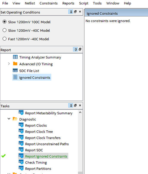
I checked the ignored constraints report in Timing analyser. It shows no constraints are ignored. See screenshot below:
But the warning: "Warning (332060): Node: WRN was determined to be a clock but was found without an associated clock assignment." still remains. Just to remind you, I am not using edges of WRN to latch data. I do not understand why WRN is considered as a clock even though I am not coding it as a clock.
Thank you!
- 신규로 표시
- 북마크
- 구독
- 소거
- RSS 피드 구독
- 강조
- 인쇄
- 부적절한 컨텐트 신고
Hi Naveen,
Speaking of legacy, you must be using the snippet to previous Quartus. What Quartus you are using now and prior to this? Can you try to use latest release and see if there is clock warning?
- 신규로 표시
- 북마크
- 구독
- 소거
- RSS 피드 구독
- 강조
- 인쇄
- 부적절한 컨텐트 신고
Hi SyafieqS_Intel,
I am using Quartus 20.1.1 Standard. All the information/code and screenshots I have shared are from the same version.
The legacy design was developed in MAXPLUS II.
Thank you.
- 신규로 표시
- 북마크
- 구독
- 소거
- RSS 피드 구독
- 강조
- 인쇄
- 부적절한 컨텐트 신고
Hi Naveen,
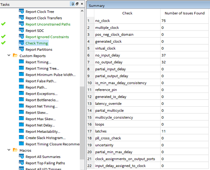
Can you click on check timing report and see if there is no clock report. You can see details of the no clock ignored as the warning mentioned that. You can see the target node of the clock with reason.
- 신규로 표시
- 북마크
- 구독
- 소거
- RSS 피드 구독
- 강조
- 인쇄
- 부적절한 컨텐트 신고
Hello @SyafieqS ,
Sorry for a late reply. I could not check with 21.1 STD.
But with QP20.1.1 STD, I find these results:
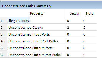
1. The two unconstrained clocks are ALE and WRN.
2. The check timing report: I guess the number 75 indicates the total number of cells which are controlled by ALE and WRN .
- 신규로 표시
- 북마크
- 구독
- 소거
- RSS 피드 구독
- 강조
- 인쇄
- 부적절한 컨텐트 신고
Hello @SyafieqS , sorry for a delayed reply. Held up with too many topics.
To replace false path to clock groups, I should first create clock constraints on WRN and ALE. This is as per Intel's example set clock groups constraint:
But since ALE and WRN are just address latch and write enable signals they do not have a clock period. So, I do not know how to write a generate clock constraint on ALE and WRN.
The below screenshot shows the behaviour of ALE and WRN during a bus write cycle:
Thank you.


